Semiconductor light emitting element

A technology for light-emitting elements and semiconductors, applied in semiconductor devices, electrical components, electro-solid devices, etc., can solve problems such as difficulties, and achieve the effects of improving light reflection, reducing element resistance, and excellent current diffusivity

Active Publication Date: 2008-08-06
NICHIA CORP
View PDF12 Cites 47 Cited by
  • Summary
  • Abstract
  • Description
  • Claims
  • Application Information

AI Technical Summary

Problems solved by technology

Especially for the latter, in order to improve the power efficiency, it is necessary to reduce the element resistance such as Vf and improve the luminous characteristics and light extraction efficiency, so it is sometimes difficult.

Method used


Image

  • Semiconductor light emitting element
  • Semiconductor light emitting element
  • Semiconductor light emitting element

Examples


Embodiment approach 1

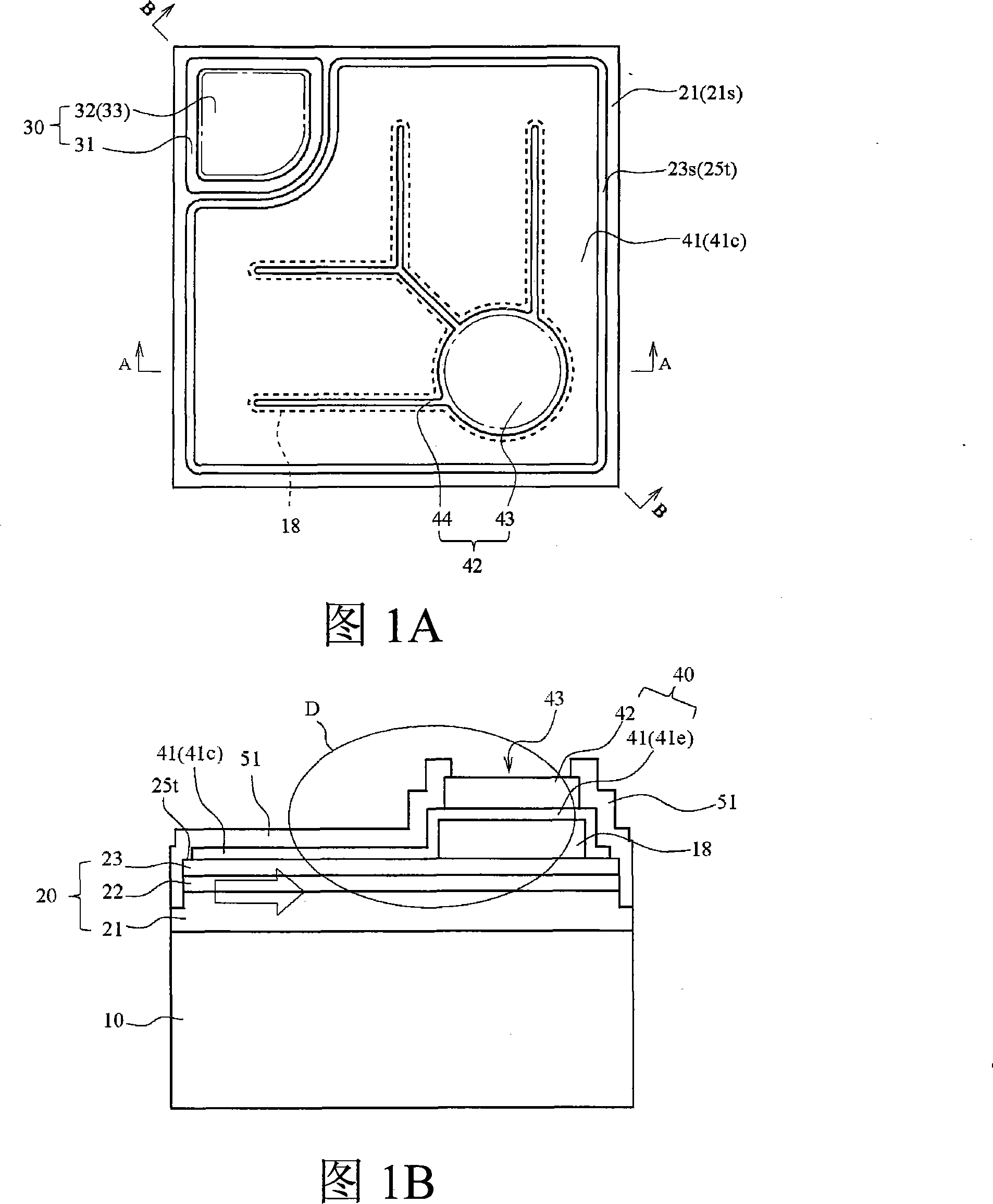
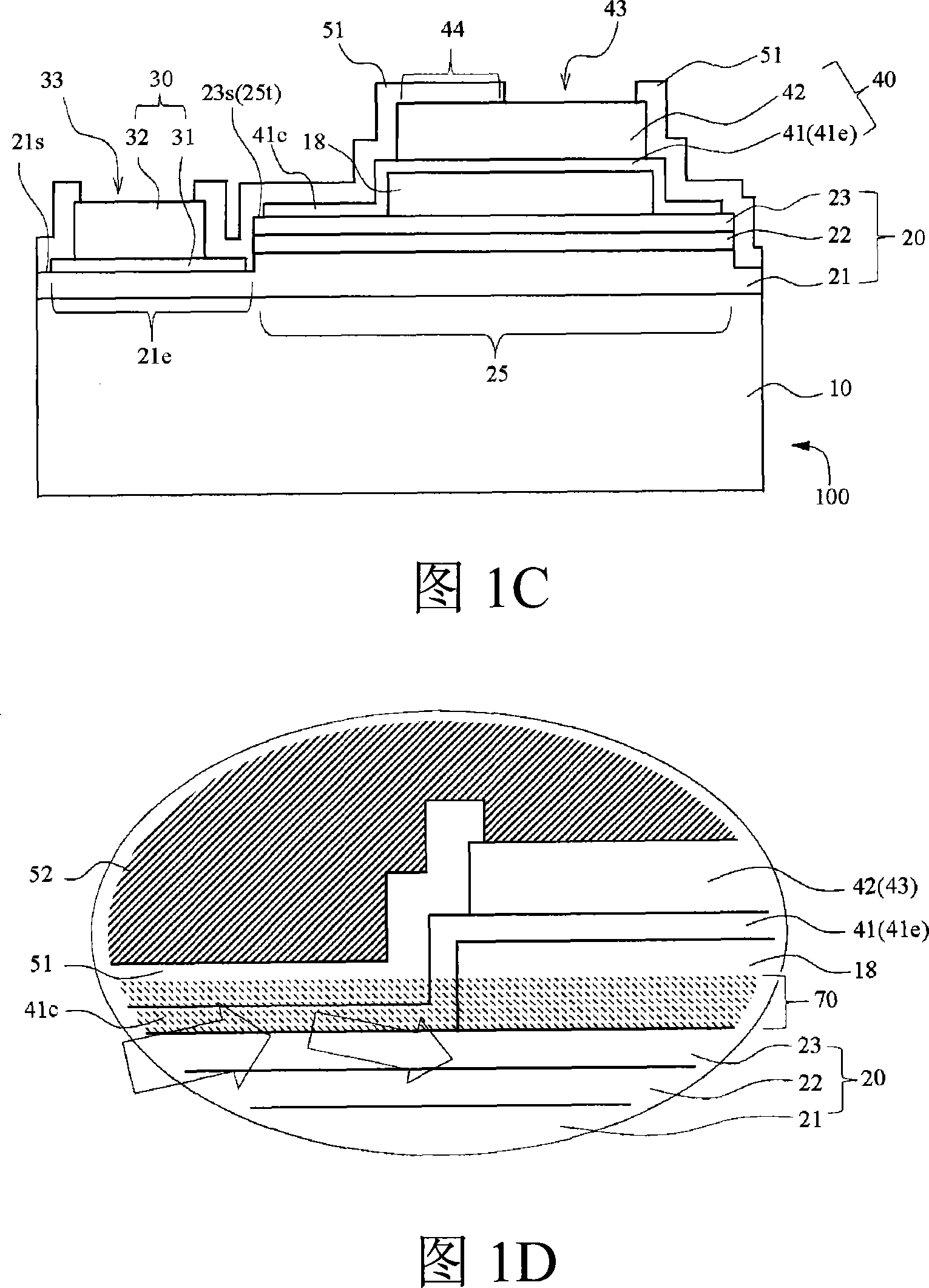
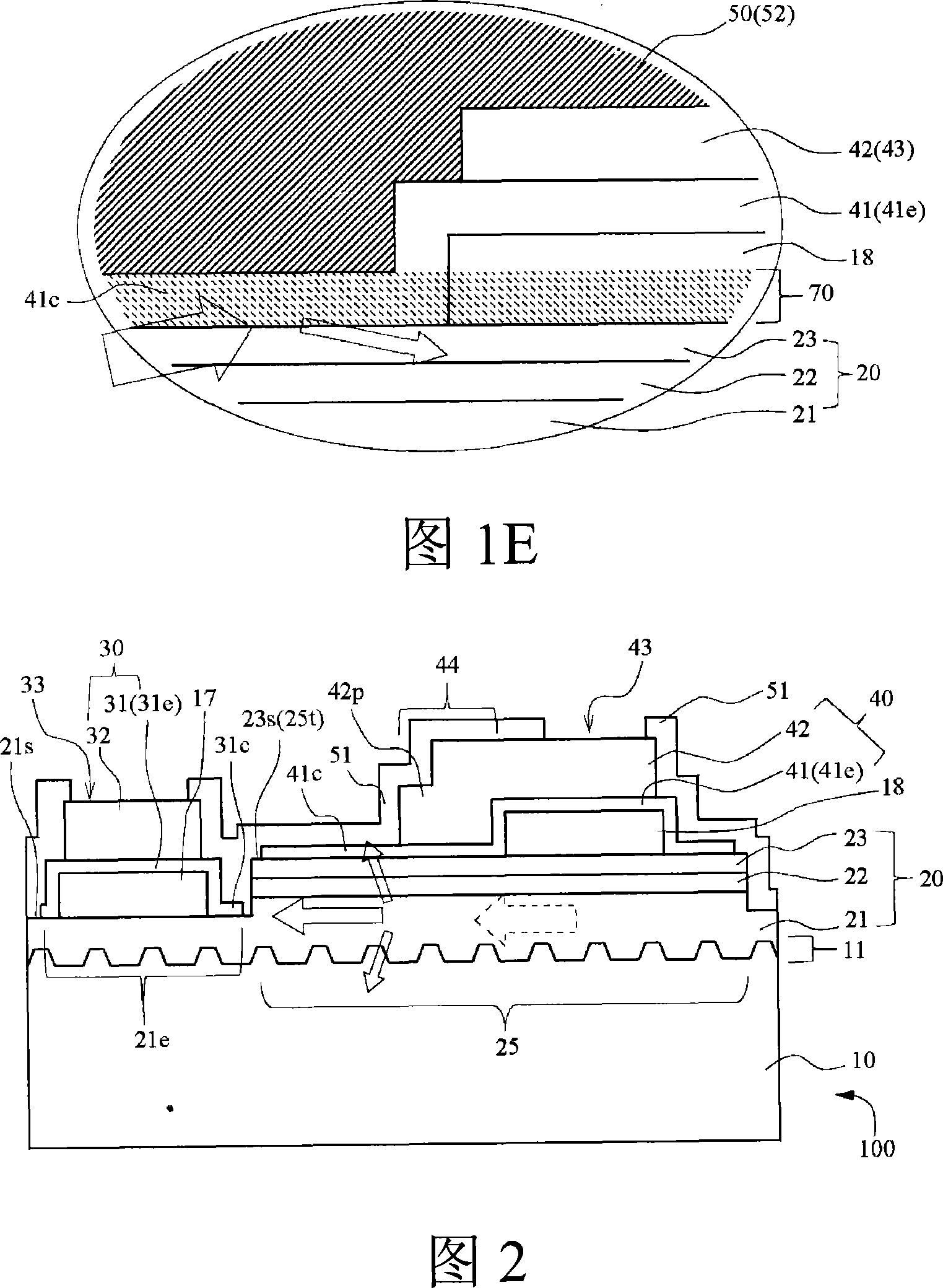
[0100]A specific example of LED100 of Embodiment 1 and its structure are demonstrated using FIG. 1. FIG. Here, FIG. 1A is a schematic diagram illustrating a plan view of the LED according to Embodiment 1 viewed from the electrode forming surface side, and FIGS. 1B and 1C are schematic diagrams illustrating cross sections along lines A-A and B-B in FIG. 1A . , FIG. 1D, FIG. 1E is a schematic diagram of FIG. 1C partially enlarged, and FIG. 1E is a schematic diagram illustrating another form of FIG. 1D.

[0101] The structure of the light-emitting element shown in FIG. 1 has a semiconductor structure 20 consisting of an n-type nitride semiconductor layer 21 in which a first conductivity type layer is laminated on a substrate 10 through a base layer (not shown) such as a buffer layer, The active layer 22 serving as the light emitting part and the p-type nitride semiconductor layer 23 of the second conductivity type layer are composed of a stacked structure, and have an element str...

Embodiment 1A

[0144] [Example 1A(1a)]2 2 2 2 <[embodiment 1C (1c)],

[0145] λ / 2n in Example 1B(1b) 2 Near, more specifically, at λ / 2n 2 ±λ / 4n 2 (λ / 4n 2 Above, 3λ / 4n 2 In the range below), better light output can be obtained. On the other hand, according to the comparison of Example 1A (1a) and Example 1C (1c), it can be seen that the thicker the insulating film, the higher the Vf tends to be. Vf becomes higher due to the first layer of the insulating film.

[0146] Next, in the above-mentioned Example 1 (research example, the structure of FIG. 1 ), the following research example, the following embodiment 2 of the second embodiment (the structure of FIG. 4 ), the embodiment 7 of the embodiment 5 (the structure of FIG. 3 structure) and the structures shown in the comparative examples of these examples, the film thickness of the first layer of ITO was changed between 20nm and 170nm to produce light-emitting elements respectively, and output characteristics as shown in FIG. 13 were obtai...

Embodiment approach 2

[0149] As Embodiment 2, in Example 1 of Embodiment 1, the shape of the extension 44 of the second electrode (p-electrode) is set to the shape shown in FIG. 4 , and the number of extensions is changed from four (Example 1 ) is set to 9 pieces, and a light-transmitting insulating film corresponding to the shape of the extension (second layer) and the electrode is provided. In addition, a substantially square (320 μm ×320μm) light-emitting element.

[0150] In this light-emitting element, compared with Example 2, the number and area of ​​electrode extensions are larger, so phenomena such as current diffusion are improved. decreased, and the output of the element tended to be slightly lower than in Example 2.

[0151] Concretely, for comparison, in the same manner as the study examples of Example 1 (Examples 1A to 1C, 1a to 1c), under the condition that the second layer of the second electrode and the light-transmitting insulating film are approximately the same area , and the s...


PUM


Abstract

The present invention provides a semiconductor light emitting element realizing lower resistance, higher output, higher power efficiency, higher mass productivity and lower cost of the element using a light transmissive electrode for an electrode arranged exterior to the light emitting structure. A semiconductor light emitting element including a light emitting section, a first electrode, and a second electrode on a semiconductor structure including first and second conductive type semiconductor layers, the first and the second electrodes being arranged on the first conductive type semiconductor layer and a second conductive type semiconductor layer of the light emitting section, respectively; and a light transmissive insulating film formed on at least one part of the second conductive type semiconductor layer; wherein the second electrode includes a first layer of a light transmissive conductive film for covering at least one part of the second conductive type semiconductor layer and a second layer which is arranged on at least one part of the light transmissive insulating film and which conducts to the first layer; a light reflecting part is formed on a surface side of the first layer, and aboundary region of the light transmissive insulating film and the semiconductor structure; and the second layer side surface of the light transmissive insulating film is distant from the semiconductor structure than the surface of the first layer.

Description

technical field [0001] The present invention relates to a semiconductor light-emitting element, in particular to an electrode structure of a light-emitting element. Background technique [0002] For light-emitting devices using nitride semiconductors, various studies have been conducted in order to obtain light emission in the near-ultraviolet to red region due to its wide bandgap characteristics. The general basic structure of a nitride semiconductor light-emitting element is a structure in which an n-type nitride semiconductor, an active layer, and a p-type nitride semiconductor are stacked on a substrate, and each layer is provided on a p-type layer and a partially exposed n-type layer. The structure of the electrode, the structure of the light-emitting element including the electrode structure is being studied. In particular, various light-emitting element structures and electrode structures have been proposed with the aim of increasing the output. [0003] Previous pr...

Claims


Application Information

Patent Timeline
Patent Type & Authority Applications(China)
IPC IPC(8): H01L33/00H01L33/06H01L33/32H01L33/38H01L33/42H01L33/44H01L33/54H01L33/56H01L33/62
CPCH01L2224/32245H01L2224/48091H01L2224/73265H01L2224/48257H01L2224/48247H01L2224/48465H01L2924/01322H01L2224/49107H01L2924/3025H01L2924/00014H01L2924/00H01L2924/00012
Inventor 佐野雅彦坂本贵彦榎村惠滋家段胜好
Owner NICHIA CORP
Why Eureka
Try Eureka