Non contact Ra radiation character etching process and its device

A non-contact, laser engraving technology, used in semiconductor/solid-state device manufacturing, electrical components, programming, etc., can solve the problem of flat corners of wafers, surface missing corners, wafer dirt and fragments, wafer fragments, etc. question

Inactive Publication Date: 2008-08-13
LITE ON SEMICON
View PDF0 Cites 2 Cited by
  • Summary
  • Abstract
  • Description
  • Claims
  • Application Information

AI Technical Summary

Problems solved by technology

[0006] (1) Since the drawn fonts and the force used cannot be effectively unified, the font size, size, and lettering depth of the specific number cannot be consistent, so the quality of the lettering cannot be effectively grasped
[0007] (2) When the force used is too large, it is not only easy to limit the number of words on the wafer, but also cause the wafer to break
[0008] (3) Due to the different hygienic habits of each operator, each operator has a different degree of cleaning when picking and placing the wafer, which makes the wafer potentially dirty and broken during the lettering process.
[0009] (4) The operator needs to directly pick and place the wafer, so it is impossible to control the cleanliness of dirt, fragments and the effective application of human force on the wafer.
[0011] However, the con

Method used


Image

  • Non contact Ra radiation character etching process and its device
  • Non contact Ra radiation character etching process and its device
  • Non contact Ra radiation character etching process and its device

Examples


Embodiment Construction

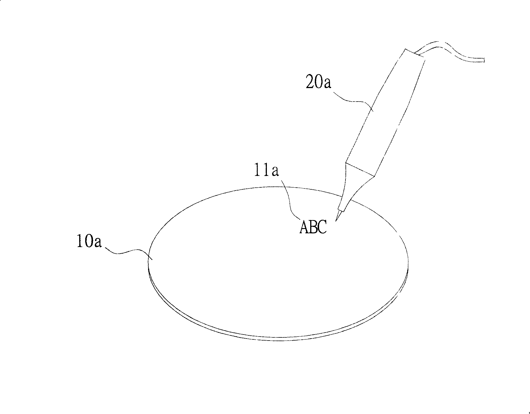
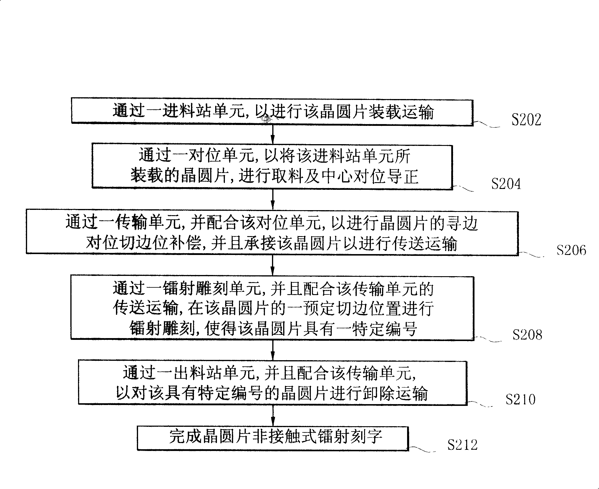
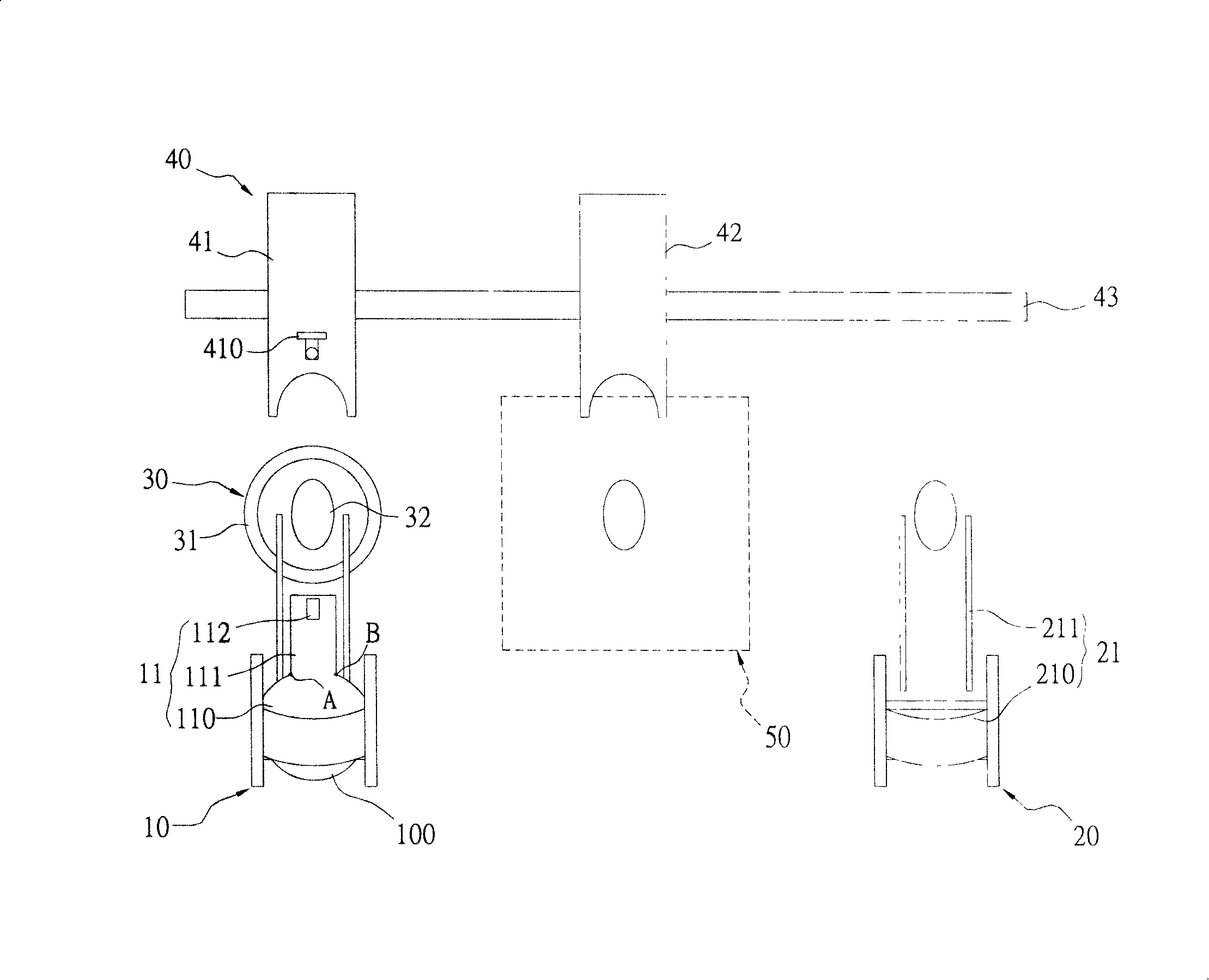
[0058] see figure 2 and image 3 As shown, it is a schematic diagram of a non-contact laser engraving process and its equipment in the present invention, which is used to laser engrave each wafer 100 to generate a specific number, and pass the specific number of each wafer 100 Numbering facilitates effective tracking management, quantity statistics and quality control during the production and transportation of the wafer 100. The steps of the non-contact laser inscription process include: first, through a feeding station unit 10, to carry out loading and transportation of the wafer 100 (S202); The wafer 100 is taken out and the center alignment is performed (S204); and then, through a transmission unit 40, and with the alignment unit 30, the edge-seeking alignment and trimming compensation of the wafer 100 is performed. And accept the wafer 100 for transport (S206); then, through a laser engraving unit 50, and cooperate with the transport of the transport unit 40, laser engr...


PUM


Abstract

A non-contact laser engraving process and device thereof, by means of contraposition guide of an edge searching contraposition module, to make the central point of a crystal wafer to contraposition to the edge searching controposition module accurately, and by the edge searching rotation of the contraposition as well as light sensing of a transmission mechanism module, to make the transmission mechanism module to intercept the central point of the crystal wafer accurately, and to locate specified edge-cutting position by the compensation of light sensor. Thus, by means of the combination of the transmission mechanism module and the laser engraving unit, even though the diameters of the engraved crystal wafers are not same, it is also able to implement laser engraving at a specified edge-cutting position of the crystal wafer accurately, and make the crystal wafer generate a specified serial number so as to bring convenience to production, also it is convenient to implement tracing management, quantity statistics and quality control management when transporting the crystal wafer, so as to improve available control management and statistics of the crystal wafer quality fine rate.

Description

technical field [0001] The present invention relates to a non-contact laser engraving process and its equipment, especially to an alignment guide through an edge-finding and alignment module, which is matched with a transmission mechanism module to achieve an edge-finding and compensation sensing mechanism. A predetermined position is formed on the wafer, so that the laser engraving unit can form a non-contact laser engraving process and equipment for a specific number at the predetermined position. Background technique [0002] In a modern society with ever-changing science and technology, various technological products used for information communication are becoming more and more complicated, and various electronic and mechanical components used in these technological products become these technological products. Is it possible to Pushers with diversified functions, among which, in most electronic or automation products, most of them contain control chips as the most impor...

Claims


Application Information

Patent Timeline
IPC IPC(8): H01L21/00B41M5/24
Inventor 黄宗健田家宏李训敏
Owner LITE ON SEMICON
Why Eureka
Try Eureka