Square flat non-connection pin multi-chip encapsulation structure

A multi-chip packaging, square flat technology, applied in the direction of electrical components, electrical solid devices, circuits, etc., can solve the problems of difficult manufacturing, high cost, and large overall thickness of the packaging structure, and achieve small packaging thickness, simple structure, and space improvement The effect of utilization

Inactive Publication Date: 2008-08-13
ADVANCED SEMICON ENG INC
View PDF3 Cites 18 Cited by
  • Summary
  • Abstract
  • Description
  • Claims
  • Application Information

AI Technical Summary

Problems solved by technology

However, its disadvantage is that it still needs to use a substrate with a complex structure, which is not only difficult to manufacture and high in cost, but also the overall thickness of the packaging structure is relatively large.

Method used


Image

  • Square flat non-connection pin multi-chip encapsulation structure
  • Square flat non-connection pin multi-chip encapsulation structure

Examples


Embodiment Construction

[0020] Relevant detailed description and technical contents of the present invention are as follows now in conjunction with the accompanying drawings:

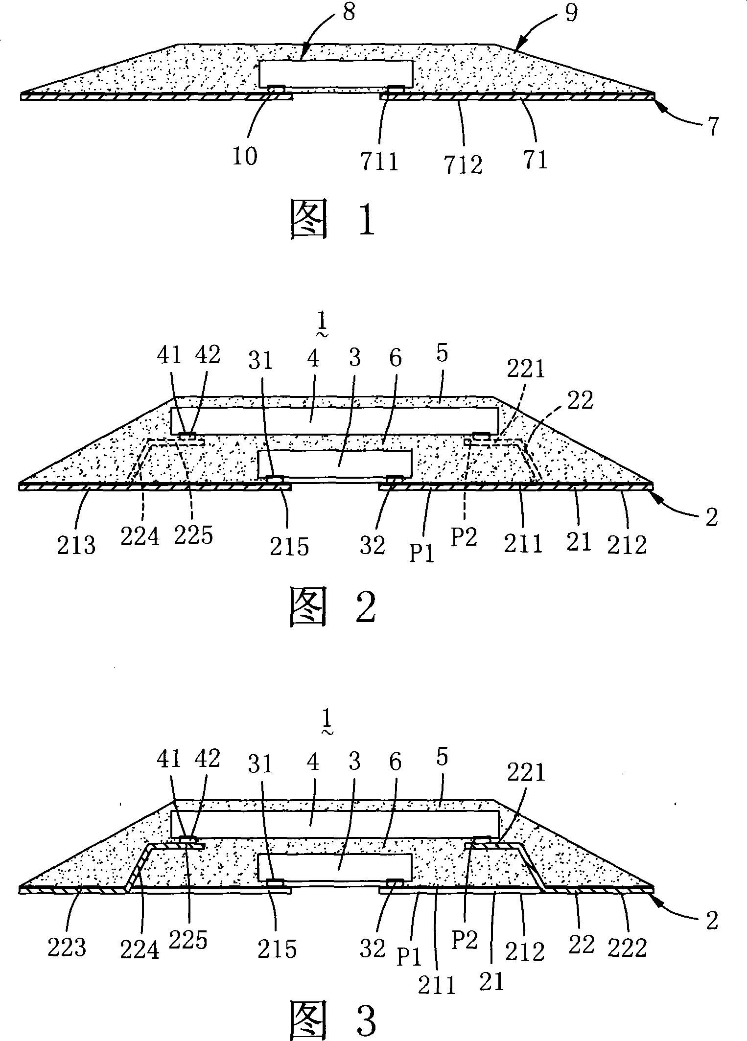
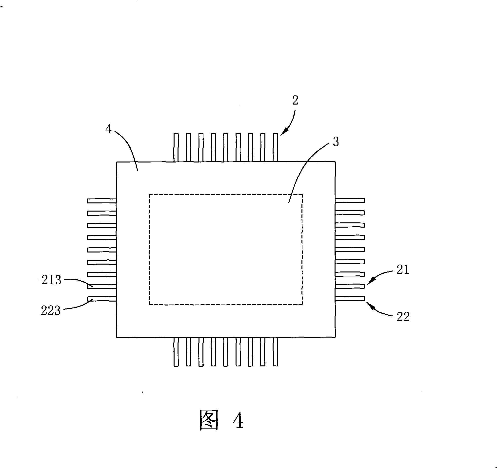
[0021] The invention discloses a quad flat no-pin (QFN) multi-chip packaging structure. Please refer to FIG. 2, FIG. 3 and FIG. 4, wherein FIG. 2 is a schematic cross-sectional view of a square flat non-pin multi-chip package structure according to a specific embodiment of the present invention, and FIG. FIG. 4 is a top view of the chip and lead frame stacking structure of the multi-chip packaging structure of the present invention. As shown in FIG. 2 and FIG. 3 , the quadrilateral flat leadless multi-chip package structure 1 of the present invention mainly includes a lead frame 2 , a first chip 3 , a second chip 4 and an encapsulant 5 .

[0022] The lead frame 2 has a plurality of first pins 21 and a plurality of second pins 22 extending on different planes, wherein each first pin 21 has a first upper surface 211 and a first...


PUM


Abstract

The invention provides a low profile quad flat and no pin type multi-chip packaging structure comprising a lead frame, a first chip, a second chip and an adhesive body. The lead frame has a first pin and a second pin that are dislocating arranged. Each first pin includes a first external portion and a first finger portion. Each second pin includes a second external portion, a bending portion and a second finger portion, wherein the bending portion bends upward so that the second finger portion of the second pin forms a height difference with the first finger portion of the first pin. The first chip locates between these first pins and these the second pins, and the second chip locates above the first chip. The adhesive body covers the first chip, the second chip, the first pin and the second pin, and manifests the lower surface of the first pin and the second pin.

Description

technical field [0001] The invention relates to a multi-chip packaging structure, in particular to a quad-flat non-leaded (QFN, Quad-Flat Non-leaded) multi-chip packaging structure. Background technique [0002] U.S. Patent No. 6,075,284 discloses an existing stacked semiconductor package structure, in which the inner pins of the lead frame respectively extend a pair of protrusions upwards and downwards to form a package structure that can be stacked upside down, but this specific It is very difficult to manufacture the shape of the lead frame no matter by embossing or stamping. In addition, the inner pins of the lead frame are located on both sides of the package structure, which belongs to a low-pin-count dual-in-line package (Dual-in-line Package, DIP), which cannot be used like a quad flat package (Quad Flat Package, QFP) package chips with more terminals. [0003] In the quad flat package structure, according to the shape of the external pins, it can be divided into I...

Claims


Application Information

Patent Timeline
Patent Type & Authority Applications(China)
IPC IPC(8): H01L25/00H01L25/065H01L23/495H01L23/31
CPCH01L2224/16245
Inventor 鲍治民
Owner ADVANCED SEMICON ENG INC
Why Eureka
Try Eureka