Tool with sintered body polishing surface and method of manufacturing the same
A technology of grinding tools and manufacturing methods, which is applied to manufacturing tools, grinding devices, grinding machine tools, etc., can solve the problem of uneven fixed installation strength of abrasive particles on substrates, and achieve high fixed installation strength and increased fixed installation strength. , to eliminate the effect of falling off
- Summary
- Abstract
- Description
- Claims
- Application Information
AI Technical Summary
Problems solved by technology
Method used
Image
Examples
Embodiment 1
[0106] A grinding tool 1 having a structure schematically shown in FIG. 1 was fabricated. A PCD block with a diameter of 90 mm integrated by simultaneous sintering of a 0.6 mm-thick sintered diamond layer and a cemented carbide was used as a tool material.
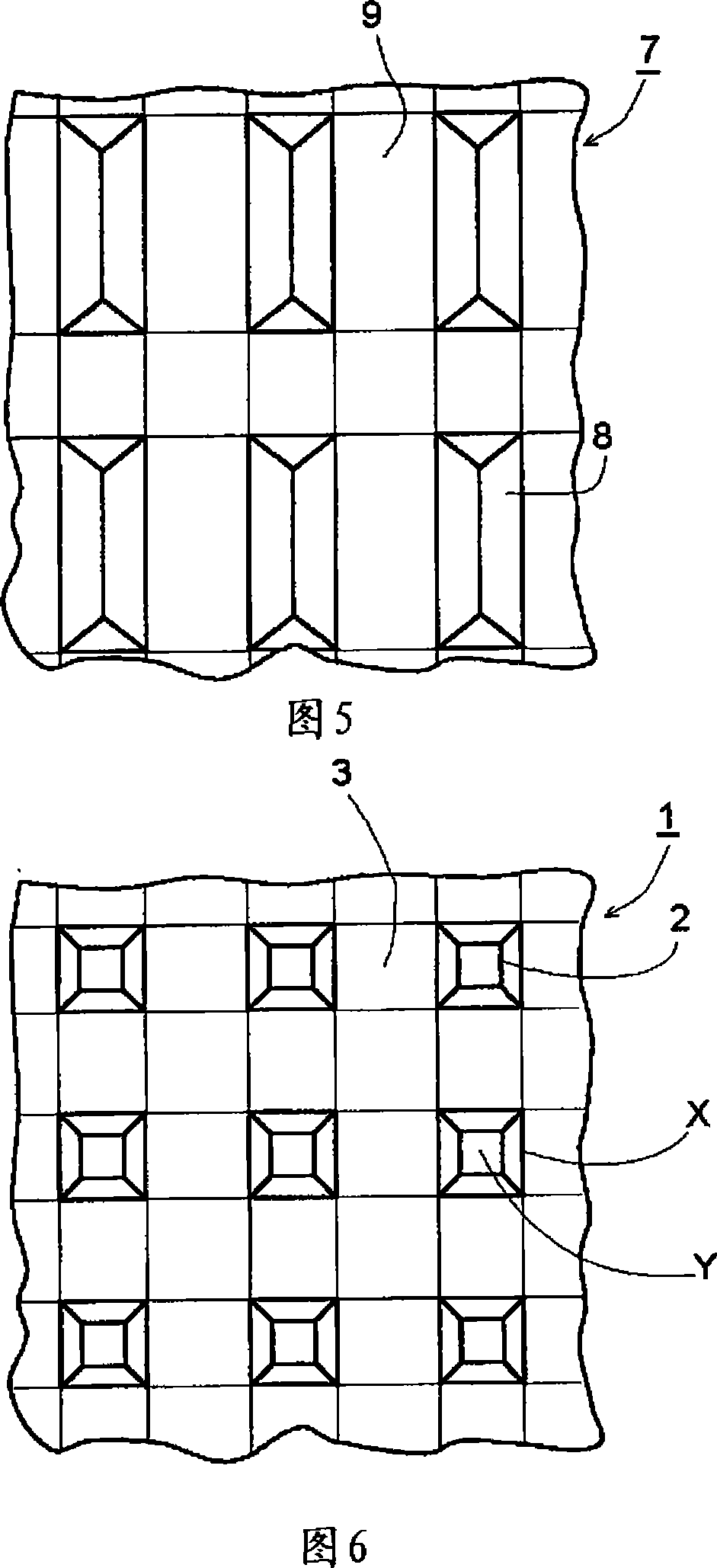
[0107] The surface of the sintered diamond layer is flattened by electric discharge machining (EDM) on the above-mentioned PCD block, and a square with a side length of 260um is formed by engraving parallel linear grooves 3 with a width of 560um by wire-cut electric discharge machining The top of the grinding unit 2. In this case, the area of the top (not shown) of the polishing unit 2 corresponds to about 10% of the cross-sectional area of the superabrasive sintered layer excluding the peripheral portion (portion of the groove 3).
[0108] Sharpening is performed on the top edge and used as a CMP dresser.
Embodiment 2
[0110] An annular grinding tool 4 schematically shown in FIG. 2 was produced. From the PcBN block integrated with the sintered c-BN layer with a thickness of 0.6mm through simultaneous sintering with the hard alloy, four 90-degree sectors with an outer radius of 60mm and an inner radius of 24mm were cut out by wire-cut EDM, as Tool raw materials.
[0111] The above-mentioned sectors are attached to a SUS-based stainless steel substrate to form a complete circle. The surface of the sintered diamond layer was ground to make it flat, and a group of parallel linear grooves 6 with a width of 560 μm was used to form a grinding unit 5 having a top of an equilateral triangle with a side length of 350 μm by wire-cut electric discharge machining. In this case, the area of the top of the grinding unit was 7% of the entire superabrasive sintered layer.
[0112] The obtained tool was sharpened in the same manner as in Example 1, and used for polishing the surface of a silicon wafer.
Embodiment 3
[0114] An abrasive tool having a structure schematically shown in FIG. 12 was fabricated. A diamond sintered body with a diameter of 100mm is used as a grinding part, and a PCD layer with a thickness of 0.5mm composed of diamond particles with a nominal particle size of 40-60um and a superhard alloy (WC-8%Co) are simultaneously sintered and integrated. Oxygen resin adhesive is fixedly installed on a SUS316 stainless steel circular substrate with a diameter of 108mm.
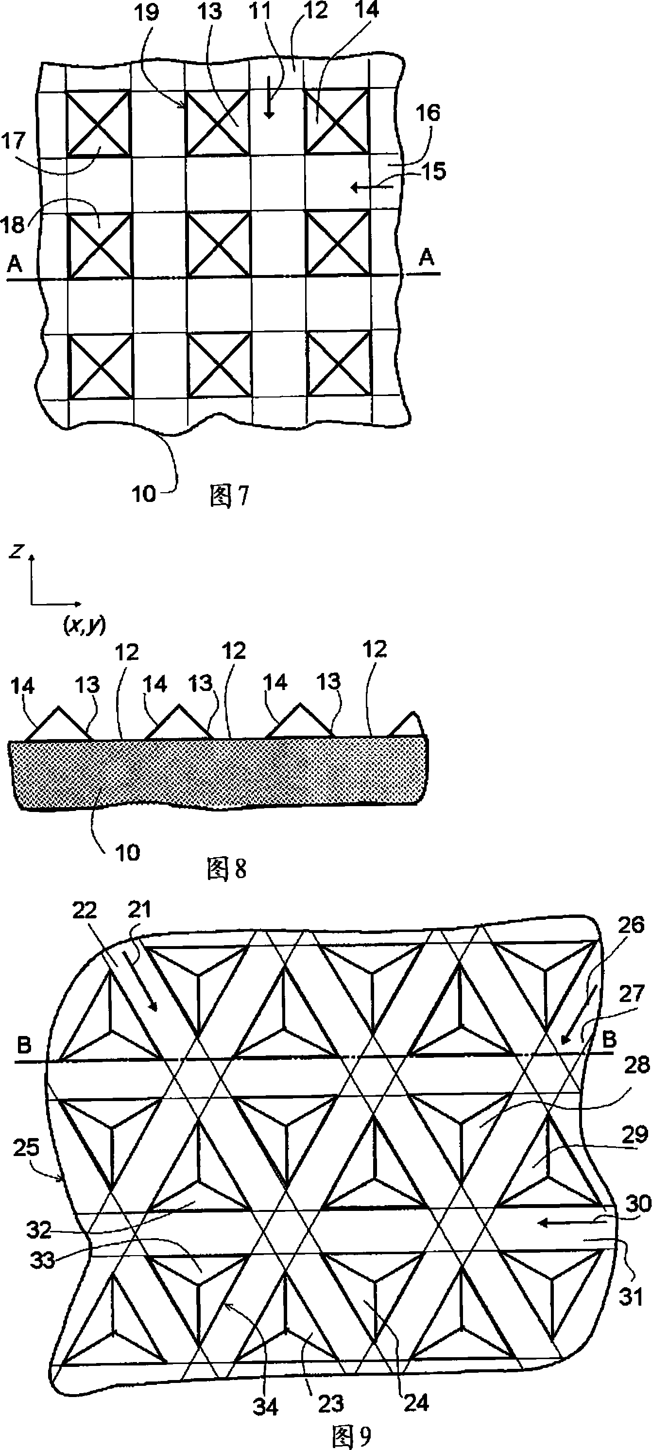
[0115] Next, after the surface of the PCD layer was planarized by die electric discharge machining, the PCD layer was cut by wire-cut electric discharge machining to form a linear groove with a width of 200um passing through the center of the raw material. In addition, the metal wire is driven sideways or moved away from the substrate (Z direction) to form a groove with a desired width and cut out the side surface of the cone.
[0116] By repeating this operation, a group of parallel grooves with a groove interv...
PUM
| Property | Measurement | Unit |
|---|---|---|
| thickness | aaaaa | aaaaa |
| diameter | aaaaa | aaaaa |
| thickness | aaaaa | aaaaa |
Abstract
Description
Claims
Application Information
 - R&D
- Intellectual Property
- Life Sciences
- Materials
- Tech Scout
- Unparalleled Data Quality
- Higher Quality Content
- 60% Fewer Hallucinations
Browse by: Latest US Patents, China's latest patents, Technical Efficacy Thesaurus, Application Domain, Technology Topic, Popular Technical Reports.
© 2025 PatSnap. All rights reserved.Legal|Privacy policy|Modern Slavery Act Transparency Statement|Sitemap|About US| Contact US: help@patsnap.com


