
Liquid crystal display device

A technology of liquid crystal display device and liquid crystal display panel, which is applied to static indicators, nonlinear optics, instruments, etc., and can solve the problems of blurred, difficult, and insufficient writing of moving images.

Active Publication Date: 2008-08-27
HITACHI DISPLAYS +1
View PDF1 Cites 3 Cited by
  • Summary
  • Abstract
  • Description
  • Claims
  • Application Information

AI Technical Summary

Problems solved by technology

[0007] In the existing black insertion display technology, when the frame rate is increased in order to improve the blurring of moving images and prevent flickering, the selection time of each scanning line is shortened, thus shortening the conduction time of the transistors connected to each scanning line. Therefore, it becomes difficult to sufficiently charge (write) the pixel electrode to a desired video voltage, and, due to insufficient writing, there is a problem that luminance inclination or display unevenness tends to occur.
[0008] On the other hand, when the output voltage of the drive circuit is increased as a whole to compensate for insufficient writing, the power consumption increases, or the operating frequency of the drive circuit as a whole increases due to an increase in the frame rate, thereby reducing power consumption. growing problem

Method used


Image

  • Liquid crystal display device
  • Liquid crystal display device
  • Liquid crystal display device

Examples


Embodiment 1

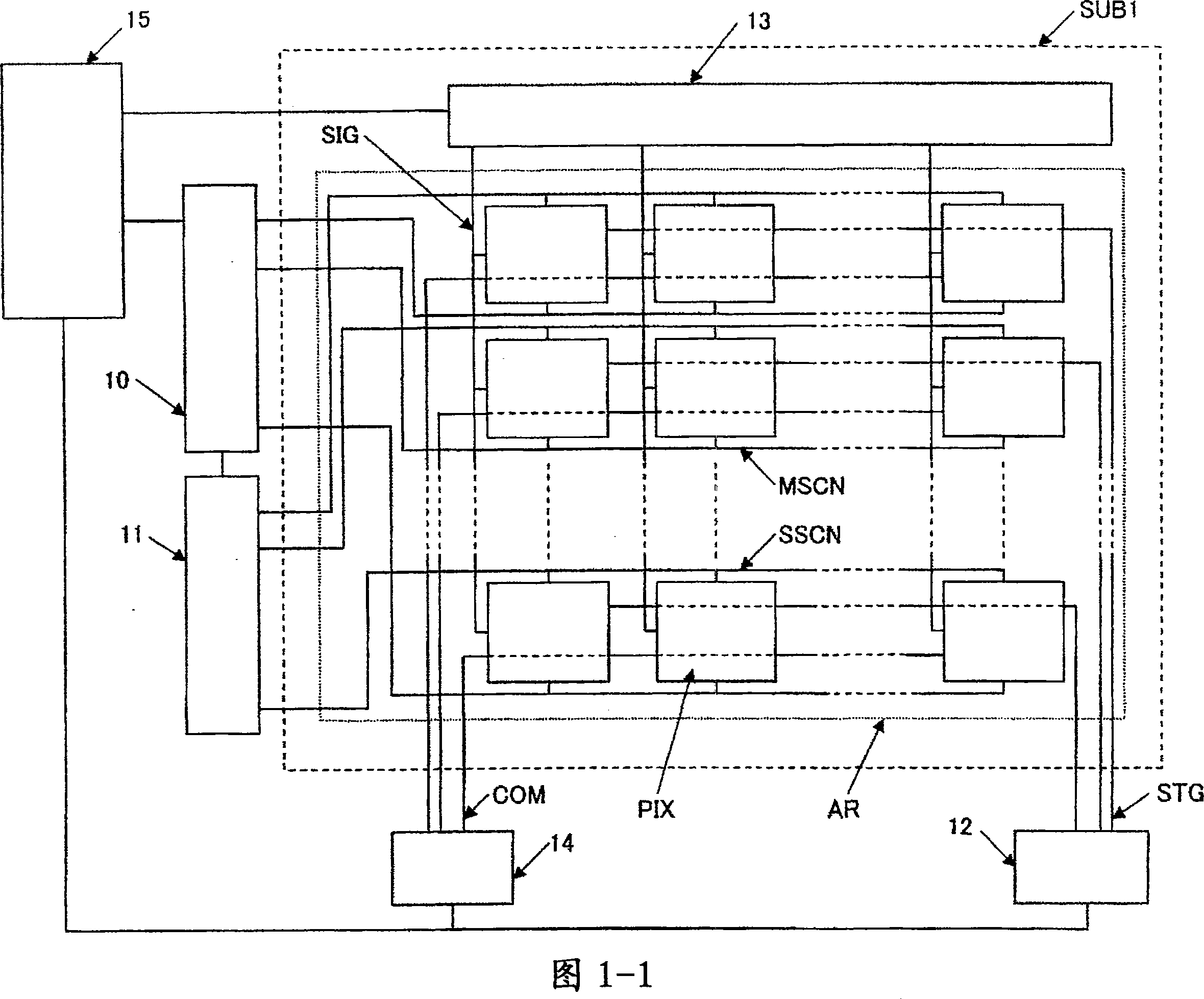
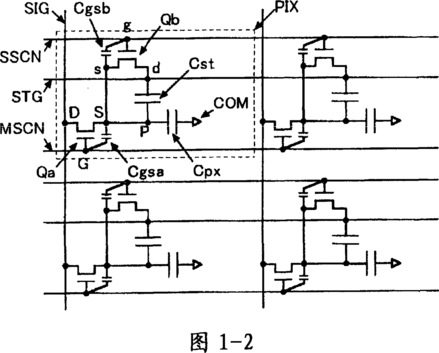
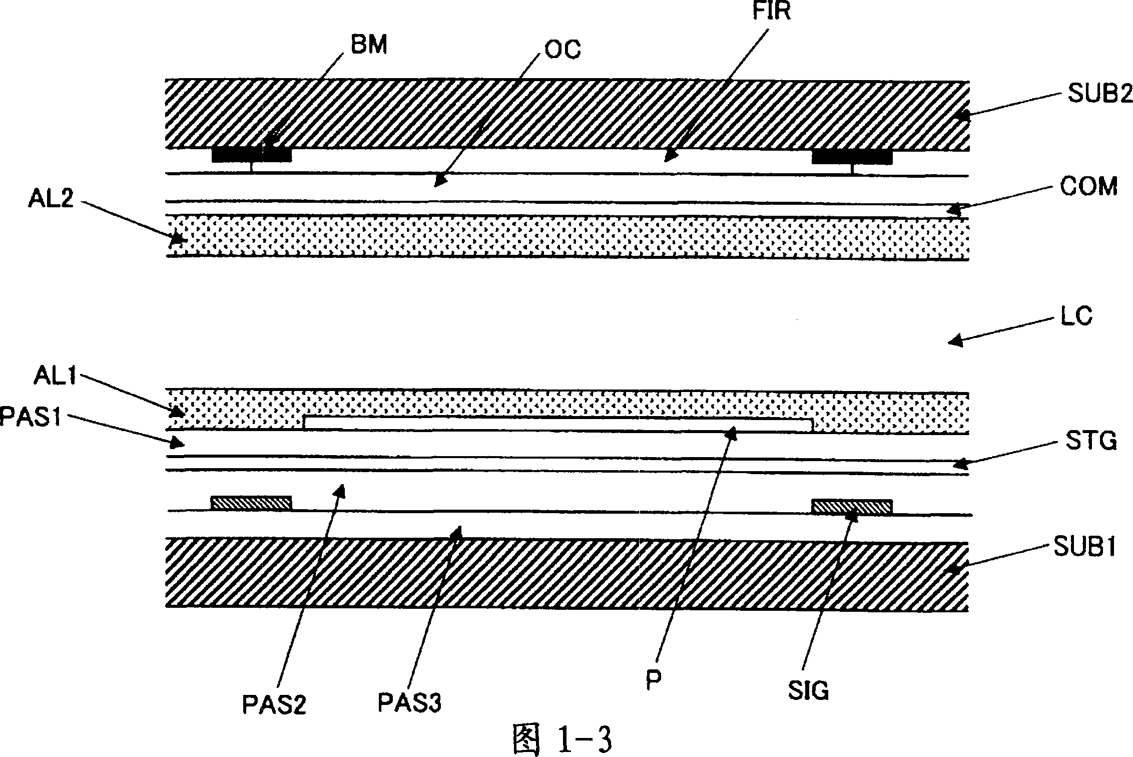
[0077] 1-1 is a diagram showing a schematic structure of a liquid crystal display device according to Embodiment 1 of the present invention, and FIG. 1-2 is a diagram showing an equivalent circuit of a pixel structure of a liquid crystal display device according to Embodiment 1 of the present invention. FIG. 1- 3 is a sectional view of main parts showing a schematic structure of the liquid crystal display panel according to Embodiment 1 of the present invention.

[0078] The liquid crystal display device of this embodiment is an active matrix liquid crystal display device using thin film transistors (TFTs). As shown in Figures 1-3, the liquid crystal display panel of this embodiment has a first substrate (SUB1), a second substrate (SUB2), and a substrate sandwiched between the first substrate (SUB1) and the second substrate (SUB2). Liquid crystal layer (LC). In this embodiment, the second substrate (SUB2) is on the observer side.

[0079] On the second substrate (SUB2), from...

Embodiment 2

[0117] The liquid crystal display device according to the second embodiment of the present invention has the same structure as the first embodiment described above except that the driving voltage waveform is different.

[0118] FIG. 3 shows driving voltage waveforms of each part in the liquid crystal display device of Example 2. In FIG. Fig. 3 (a) shows the driving voltage waveform of the first display line of the start picture scanning, Fig. 3 (b) shows the driving voltage waveform of the second display line, and Fig. 3 (c) shows the Nth display of the end picture scanning The driving voltage waveform of the row. Compared with FIG. 2-1 in the first embodiment described above, the driving voltage waveform is different at the start timing of each scanning period.

[0119] Take Figure 3(a) as an example for illustration. The first period in which the first display line, which is the first display line of the picture, starts at the same time as the scanning of the picture of th...

Embodiment 3

[0128] The liquid crystal display device of Embodiment 3 of the present invention has the same structure as that of Embodiment 1 or Embodiment 2, except that the driving voltage waveform is different.

[0129] The driving voltage waveforms of the respective parts in the liquid crystal display device of the third embodiment are shown in FIG. 4-1. Fig. 4-1(a) shows the driving voltage waveform of the first display row for starting picture scanning, and Fig. 4-1(b) shows the driving voltage waveform of the second display row.

[0130] Compared with Figure 2-1 in Example 1 and Figure 3 in Example 2, the differences are as follows. Firstly, the second period is only composed of period [3] and period [3]', and in the second period, the sub-scanning line (SSCN) of each display row is kept in the original selection state and the sub-thin film transistor (Qb) is continuously activated. ground remains on.

[0131] Vst=Vcom ................(2)

[0132] In addition, as shown in the abo...


PUM


Abstract

The present invention provides a liquid crystal display device, capable of implementing black insertion display without increasing power. The liquid crystal display device includes a liquid crystal display panel provided with plural sub-pixels, plural video wirings for inputting the video voltage to the sub-pixels, plural main-scanning wirings for inputting the selective scanning voltage to the sub-pixels, plural sub-scanning wirings provided corresponding to the plural the main-scanning wirings, and a retention capacity wiring. The sub-pixel includes a pixel electrode, an opposed electrode, a main transistor and a sub transistor. An opposed voltage generation circuit is provided for supplying the opposed voltage to the opposed electrode. The main transistor has a gate electrode connectedto the main-scanning wiring, a first electrode connected to the video wiring, and a second electrode connected to the pixel electrode. The sub transistor has a gate electrode connected to the sub-scanning wiring, a first electrode connected to the retention capacity wiring, and a second electrode connected to the pixel electrode.

Description

technical field [0001] The present invention relates to a liquid crystal display device, in particular to a liquid crystal display device capable of performing black insertion display by supplying a voltage of a capacitor line or a common electrode from a sub-TFT connected to a sub-scanning line to a pixel electrode. Background technique [0002] In a hold-type display device such as a liquid crystal display device (LCD), it is known to repeatedly perform a full-screen black display screen in which one frame is displayed after displaying an image of one frame, and a black display screen is inserted between images. The technology, which is visually close to a pulse-type display like a Braun tube (CRT), improves the blurring of moving images. [0003] Also, it is known that flicker (flicker) is sometimes observed due to insufficient improvement of moving image blurring in some cases according to this technique, and the frame rate is increased to 2 times or 3 times the usual, e...

Claims


Application Information

Patent Timeline
Patent Type & Authority Applications(China)
IPC IPC(8): G09G3/36G02F1/1362
CPCG09G2300/0861G09G2300/0823G09G3/3659G09G2310/06G09G3/3696
Inventor 佐佐木亨
Owner HITACHI DISPLAYS
Learn More