Soldering circuit plate and soldering method thereof
A welding method and circuit board technology are applied in the directions of printed circuits connected with non-printed electrical components, printed circuit components, and printed circuits assembled with electrical components. 104 Fracture, virtual welding and other problems, to achieve the effect of increasing the conductive path
- Summary
- Abstract
- Description
- Claims
- Application Information
AI Technical Summary
Problems solved by technology
Method used
Image
Examples
Embodiment Construction
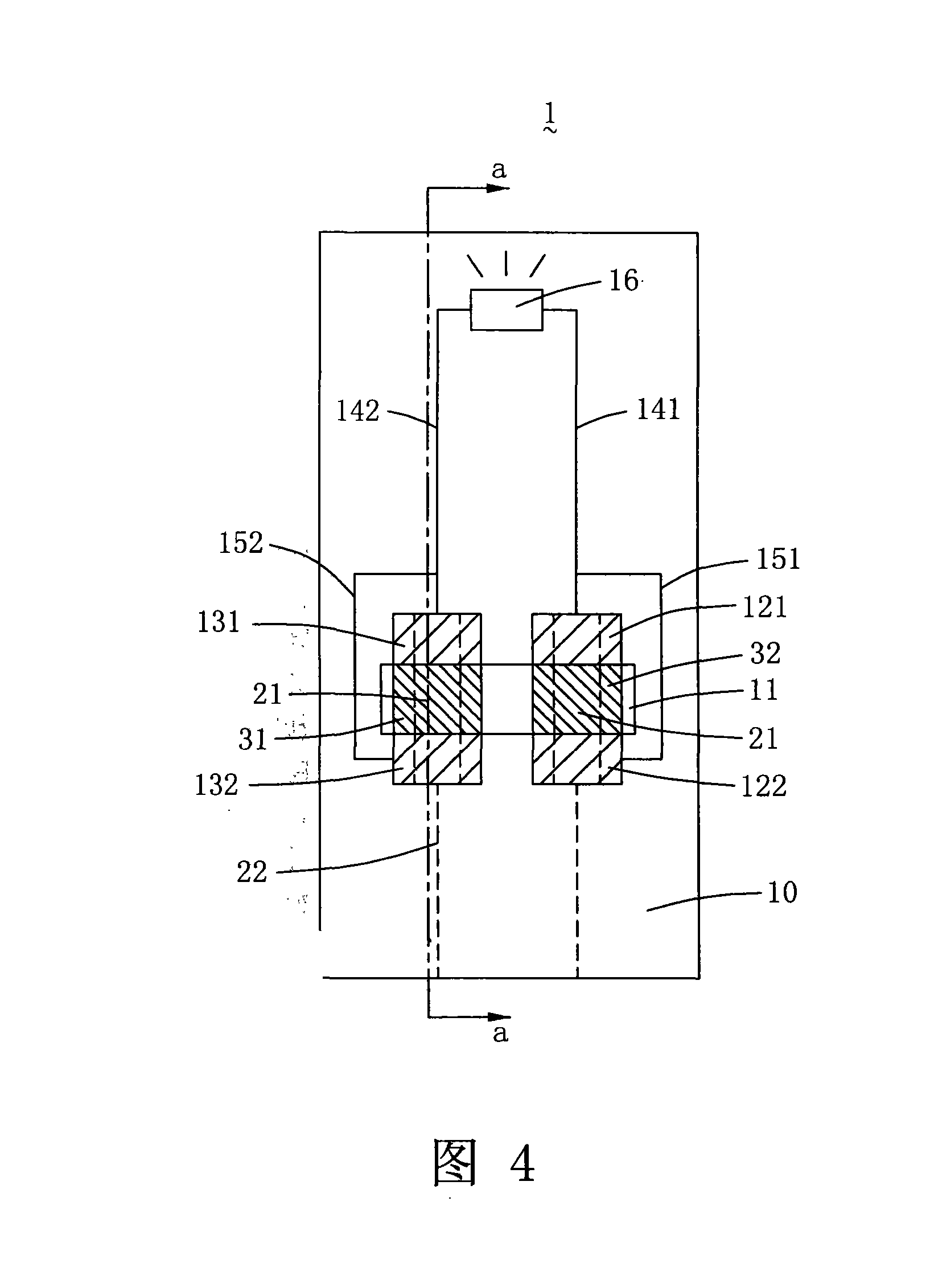
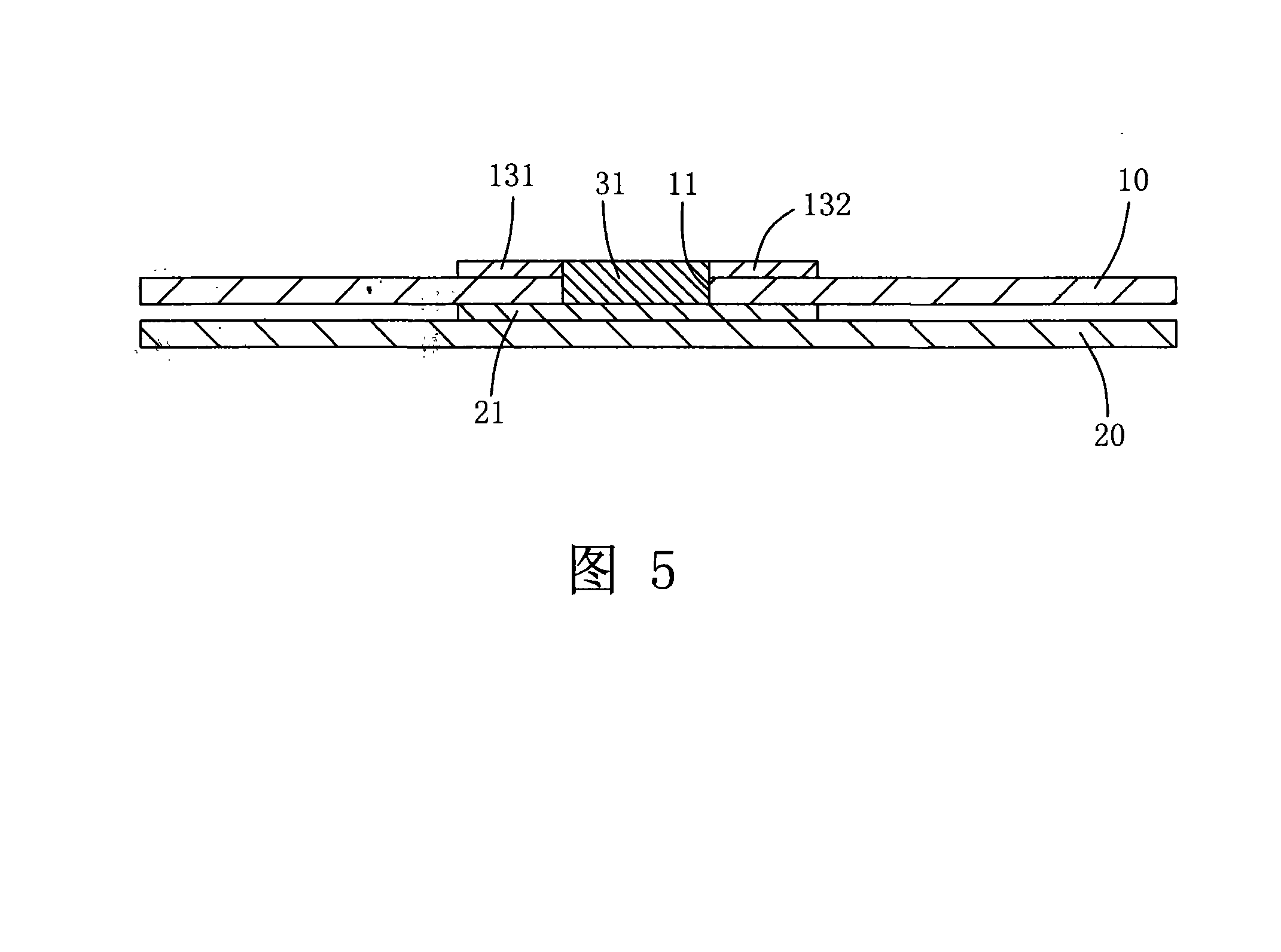
[0025] Referring to FIG. 2 and FIG. 4 , the solderable circuit board 1 according to a preferred embodiment of the present invention includes a first circuit board 10 and two pairs of first soldering pads 121 and 122 , 131 and 132 . The first circuit board 10 has a through opening 11; two pairs of the first welding pads 121 and 122, 131 and 132 are arranged side by side along the opening 11, and each pair of the first welding pads 121 and 122, 131 and 132 is formed by the opening 11. The axes are respectively arranged on two opposite sides of the opening 11 . The first welding pad 121 located on one side of the opening 11 is electrically connected to one polarity pin of an electronic component 16 (such as a light emitting diode shown in the figure) via a first conductive circuit 141 . In addition, a first external conductive circuit 151 is further provided on the first circuit board 10 , one end of the first external conductive circuit 151 is connected to the first welding pad ...
PUM
 Abstract
Description
Claims
Application Information


