Ultra wide band millimeter wave vertical interconnection structure based on HTCC

An interconnection structure and millimeter wave technology, applied in the field of radio frequency interconnection, can solve problems such as discontinuity of radio frequency signal transmission, and achieve the effects of good consistency, high reliability and easy processing

Active Publication Date: 2022-02-01
CHENGDU SEEKCON MICROWAVE COMM
View PDF7 Cites 1 Cited by
  • Summary
  • Abstract
  • Description
  • Claims
  • Application Information

AI Technical Summary

Problems solved by technology

With the increase of signal frequency and the broadening of signal bandwidth, the discontinuity of RF signal transmission in the vertical interconnection structure has become a bottleneck restricting the application of SiP in the field of ultra-high frequency and ultra-wideband

Method used


Image

  • Ultra wide band millimeter wave vertical interconnection structure based on HTCC
  • Ultra wide band millimeter wave vertical interconnection structure based on HTCC
  • Ultra wide band millimeter wave vertical interconnection structure based on HTCC

Examples


Embodiment 1

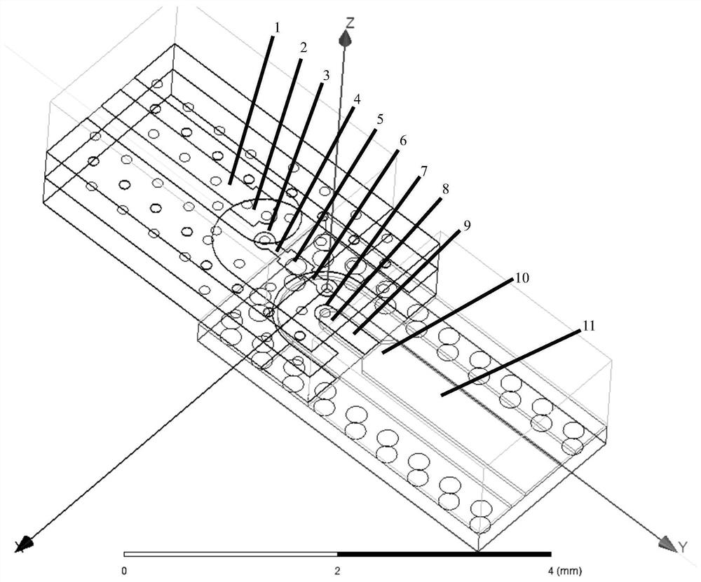
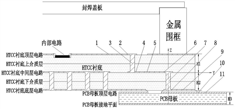
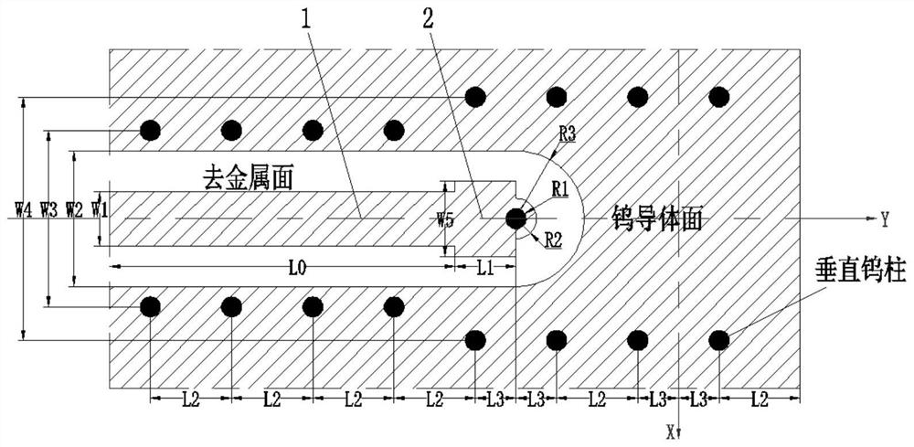
[0041] An HTCC-based ultra-wideband millimeter-wave vertical interconnection structure disclosed by the present invention, such as figure 1 as shown, figure 1 The sectional view of the middle YOZ plane is as follows figure 2 as shown, figure 2 HTCC substrate top layer circuit pattern such as image 3 as shown, figure 2 The pattern of the dielectric layer on the medium HTCC substrate is as follows Figure 4 as shown, figure 2 The circuit pattern of the middle layer of the HTCC substrate is as follows: Figure 5 as shown, figure 2 The pattern of the dielectric layer under the medium HTCC substrate is as follows Figure 6 as shown, figure 2 The underlying circuit pattern of the HTCC substrate is as follows: Figure 7 as shown, figure 2 The top layer circuit pattern of the middle PCB mother board is as follows: Figure 8 shown. The present invention achieves vertical interconnection by rationally designing the pattern of each tungsten conductor layer in the HTCC...

Embodiment 2

[0063] Such as figure 2 As shown, the present invention provides a packaging structure, including the HTCC-based ultra-wideband millimeter-wave vertical interconnection structure of Embodiment 1, a sealing cover plate and a metal enclosure, and the HTCC-based ultra-wideband millimeter-wave vertical interconnection structure is installed on the package The welding cover plate and the metal enclosure, and the sealing welding cover plate is covered in the metal enclosure.

[0064]In this embodiment, the packaging structure provided by the present invention adopts the HTCC-based ultra-wideband millimeter-wave vertical interconnection structure of Embodiment 1, which has excellent electrical characteristics such as ultra-high operating frequency, ultra-wide operating frequency band, and ultra-low insertion loss. At the same time, the interconnect structure is easy to process, has high reliability, good consistency, and strong derivability, which is very suitable for mass productio...


PUM


Abstract

The invention provides an ultra wide band millimeter wave vertical interconnection structure based on an HTCC, and belongs to the technical field of radio frequency interconnection. The vertical interconnection structure comprises an HTCC substrate and a PCB mother board. The HTCC substrate and the PCB mother board are sequentially connected in series with a transmission sub-structure which is formed by a first coplanar waveguide, a first class coaxial, a first strip line, a second class coaxial, a second strip line and a second coplanar waveguide. The invention provides the ultra wide band millimeter wave vertical interconnection structure based on a mature HTCC process technology for SIP adopting the HTCC as a substrate material, and the radio frequency vertical interconnection structure realizes excellent electrical characteristics of high working frequency, wide working frequency band, low insertion loss and the like, and has the characteristics of easiness in processing, high reliability and the like.

Description

technical field [0001] The invention belongs to the technical field of radio frequency interconnection, and in particular relates to an ultra-wideband millimeter wave vertical interconnection structure based on HTCC. Background technique [0002] In the post-Moore era, advanced semiconductor chip technology is approaching the physical limit, and System in Package (SiP) is an important realization path beyond Moore's Law. SiP is from the standpoint of packaging, packaging different chips side by side or superimposed, and preferentially assembling multiple active electronic components with different functions and optional passive devices, as well as other devices such as micro-electromechanical devices or optical devices. Together, a single standard package that implements certain functions. [0003] SIP is generally composed of a substrate, a metal frame, a sealing cover and an internal circuit (composed of interconnections of various devices). SIP is generally used on a PCB...

Claims


Application Information

Patent Timeline
Patent Type & Authority Applications(China)
IPC IPC(8): H01P5/08H01L23/66H01L23/498
CPCH01P5/08H01L23/49827H01L23/49838H01L23/66H01L2223/6616H01L2223/6627
Inventor 姚剑平孙科杨秀强杨先国李庆东李硕友杨飞
Owner CHENGDU SEEKCON MICROWAVE COMM
Why Eureka
Try Eureka