Organic el display

A display device and component technology, applied to static indicators, instruments, etc., can solve problems such as inability to realize image display and changes in luminous brightness, and achieve the effects of reducing feedback errors, stable comparison objects, and easy comparison

Active Publication Date: 2008-09-10
SAMSUNG DISPLAY CO LTD
View PDF2 Cites 19 Cited by
  • Summary
  • Abstract
  • Description
  • Claims
  • Application Information

AI Technical Summary

Problems solved by technology

Considering that the light emission of the OLED element is proportional to the current flowing through the OLED element, the luminance of the OLED element will change over time even if the same voltage is applied, and correct image display cannot be realized.

Method used


Image

  • Organic el display
  • Organic el display
  • Organic el display

Examples


Embodiment 1

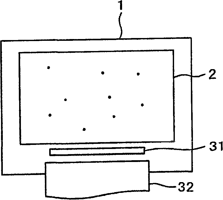
[0085] figure 1 It is an example of an organic EL display device embodying the present invention. exist figure 1 Among them, the display region 2 is formed on most of the organic EL display panel 1 . A driver IC 31 for driving the organic EL display panel 1 is provided on the lower side of the screen. On the lower side of the driver IC 31 , a flexible wiring substrate 32 is mounted on the organic EL display panel 1 . External image signals, power, and the like are supplied to the organic EL display panel 1 through the flexible wiring substrate 32 . The flexible wiring board is usually bent toward the back of the organic EL display panel and accommodated in the bezel.

[0086] exist figure 1 The display area 2 is formed with a plurality of pixels PX. However, not all pixels PX are normal, such as figure 1 Abnormal pixels as shown by a few black dots in . This portion is a portion where the OLED element does not emit light due to a short circuit or an open circuit of...

Embodiment 2

[0116] In Embodiment 1, the afterimage of the pixel PX is judged by comparing with adjacent pixels. That is, the anode voltage of the OLED element 11 of the measurement pixel is compared with the anode voltage of the OLED element 11 of the adjacent pixel. Such an evaluation method may accumulate measurement errors when comparing pixels.

[0117] As a method of preventing accumulation of errors, the present embodiment adopts the following method. The structure of the organic EL display device to which this embodiment is applied and Figure 10 Same. That is, remove the Figure 10 In addition to the data of the pixels judged to be faulty by the failure judging part 81, the data of each pixel is transmitted to the afterimage judging part 82. In the present embodiment, the afterimage determination unit 82 uses the transferred data for one line to create reference data serving as a reference for comparison. Then, by comparing the reference data with the data of each pixel, the ...

Embodiment 3

[0120] Figure 13 It is an example of the organic EL display device according to the third embodiment of the present invention. Same as embodiment 1, in this embodiment also as Figure 11 The pixels PX on the detection row of the scanning line are sequentially detected from the left as shown. However, in the present embodiment, the afterimage determination of the pixel PX is not compared with adjacent pixels, but compared with the data of the reference pixel.

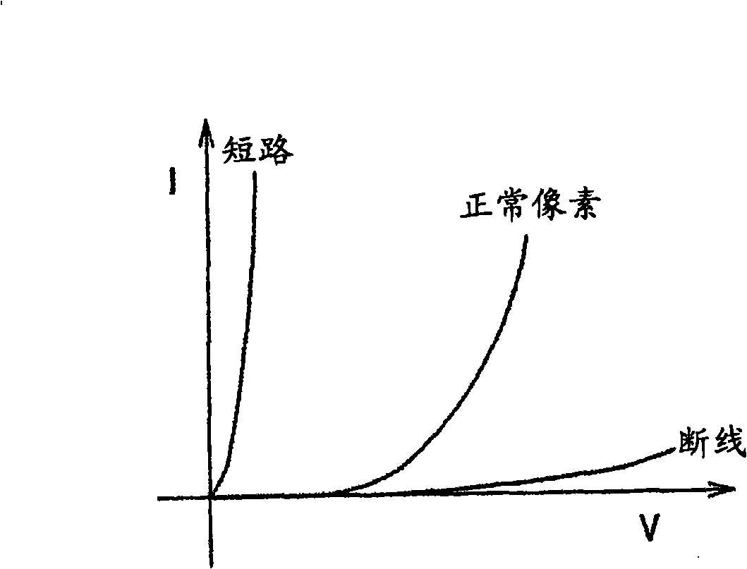
[0121] In this case, if there is an abnormality in the reference pixel, there is a risk that all the correction data cannot be used. In order to prevent this danger, it is regularly checked whether the reference pixel maintains a normal value. For example, for benchmark data as well Figure 7 As shown, the normal range and the abnormal range can be determined in advance, and when the reference pixel is outside the normal range, it is necessary to perform an operation of excluding the reference pixel. For example, a...


PUM


Abstract

The invention provides an organic EL displaying device. The afterimage phenomenon of the image can be accurately measured in the organic EL displaying device and the image data can be corrected thereby forming a correct image. The voltage-current characteristics of a special pixel (PX) are measured, and the data of line one is stored in the line memorizer (MR1). The comparison of characteristic data is executed by comparing the adjacent pixels with each other. A fault determining part (81) determines whether the pixel being compared is fault pixel, and the pixel is eliminated from comparing object if the pixel is a fault pixel. In the afterimage determining part (82), only the normal pixel is compared for obtaining the accurate afterimage data. In the calculating part (9), the afterimage data is reflected to the image data from the host computer.

Description

technical field [0001] The present invention relates to an organic EL display device, in particular to a display technology for correcting the change of the luminescent characteristics of an organic EL element with operating time. Background technique [0002] The mainstream of conventional display devices is CRT, but instead, liquid crystal display devices, plasma display devices, etc., which are flat panel display devices, are being put into practical use, and demand is gradually increasing. Furthermore, in addition to these display devices, a display device using organic electroluminescence (hereinafter referred to as an organic EL display device (OLED)) and an electron source arranged at the anode by arranging electron sources using field emission in a matrix form The development and practical use of a display device (FED display device) in which a phosphor emits light to form an image is also progressing. [0003] Organic EL display devices have the following character...

Claims


Application Information

Patent Timeline
Patent Type & Authority Applications(China)
IPC IPC(8): G09G3/30G09G3/32G09G3/20
CPCG09G3/3233G09G2300/0809G09G2320/0285G09G2320/046G09G2330/08G09G2330/10
Inventor 宫本光秀河野亨石井雅人笠井成彦秋元肇
Owner SAMSUNG DISPLAY CO LTD
Why Eureka
Try Eureka