Pixel circuit, display device, and driving method thereof

A technology for display devices and pixel circuits, applied in circuits, lighting devices, electric light sources, etc., can solve problems such as affecting luminous brightness

Inactive Publication Date: 2008-09-17
SONY CORP
View PDF2 Cites 20 Cited by
  • Summary
  • Abstract
  • Description
  • Claims
  • Application Information

AI Technical Summary

Problems solved by technology

The characteristic change of the active element used for this driving and the characteristic change of the photoelectric element will affect the luminance of light emission even in the case of the constant current driving method

Method used


Image

  • Pixel circuit, display device, and driving method thereof
  • Pixel circuit, display device, and driving method thereof
  • Pixel circuit, display device, and driving method thereof

Examples


change example

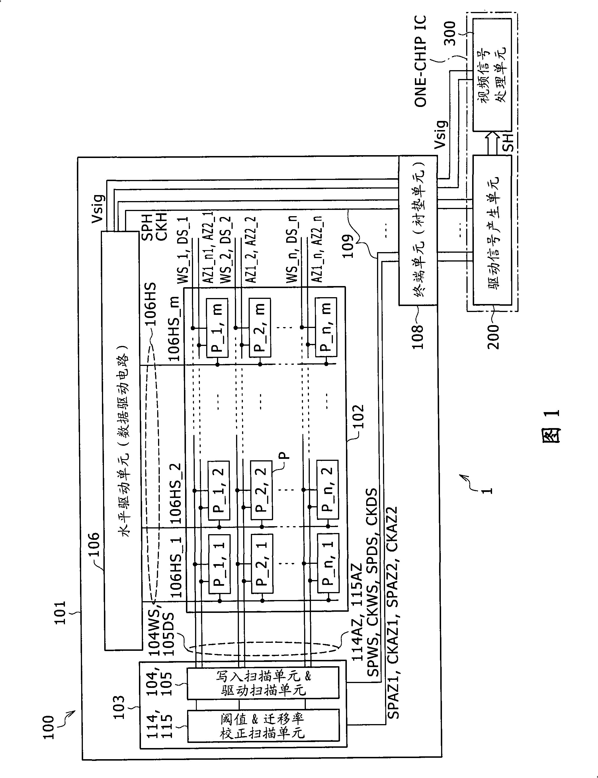
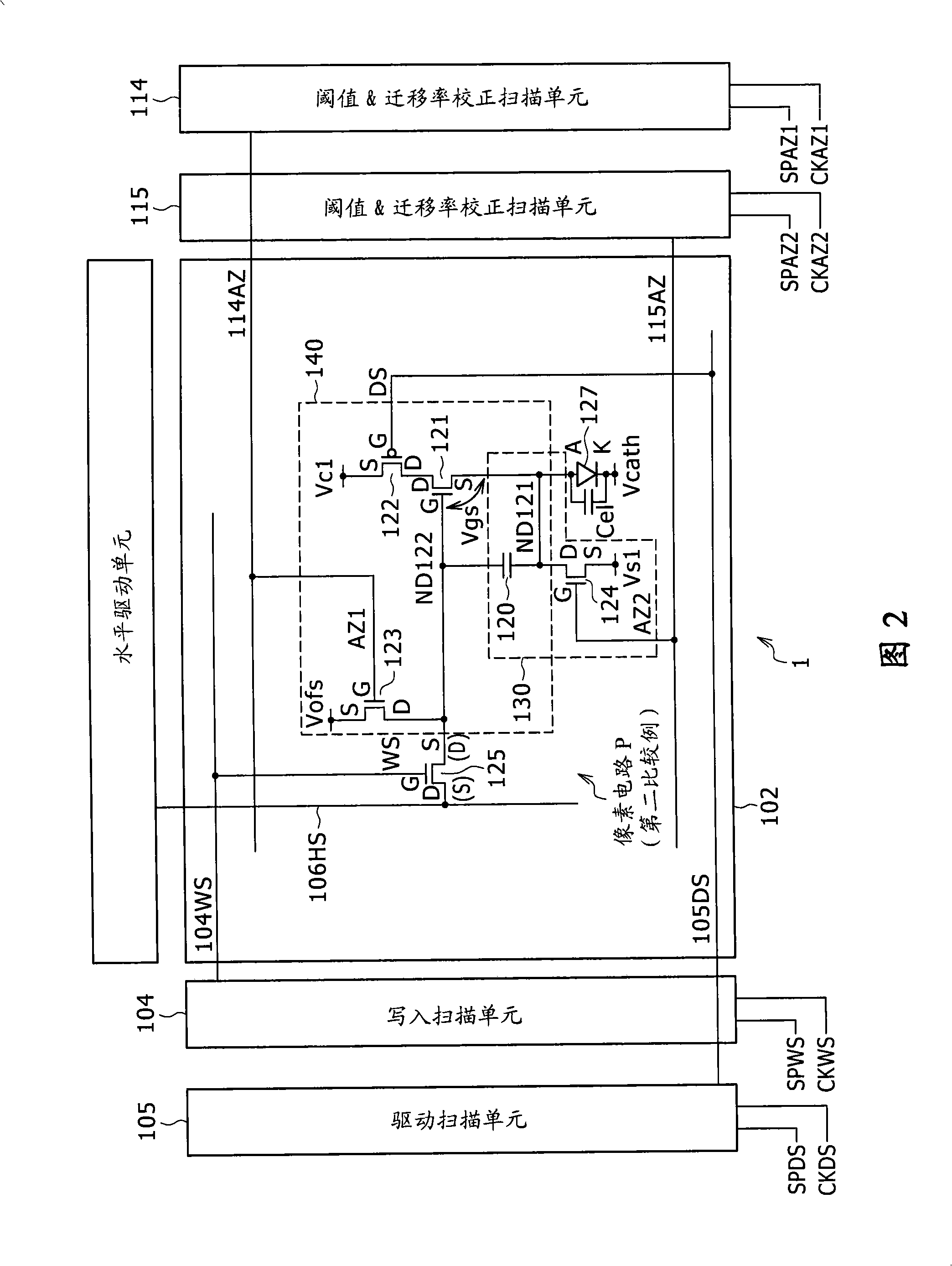
[0213] FIG. 11 is a diagram of assistance in explaining the operation of a modified example for correcting a decrease in gate-source voltage Vgs caused by mobility correction. FIG. 11 shows the DS coupling when displaying white, gray, and black in the case of combining the mechanism of changing the cut-off point of each gradation by inactivating the falling edge of the write drive pulse WS and the DS coupling. The drive pulses WS and DS drive the respective voltages on the gate and source of transistor 121 .

[0214] In the above correction mechanism, the Vgs replenishment amount is actually a constant regardless of the level. Thus, for example, black floats may occur. On the other hand, for the optimum mobility correction time for each level, there is a mechanism for changing the cutoff point for each level by inactivating the falling edge of the write drive pulse WS. The use of this mechanism can widen the gate-source voltage Vgs through DS coupling, and thereby reduce the...


PUM


Abstract

The invention discloses a pixel circuit, a display device including the pixel circuit and a method for driving the pixel circuit. The display device includes a pixel array unit and a control unit. According with the invention, brightness decrease caused by mobility correction can be avoided, and video signal size needs not increased.

Description

[0001] Cross References to Related Applications [0002] The present invention contains subject matter related to Japanese Patent Application No. JP 2007-068020 filed in the Japan Patent Office on Mar. 16, 2007, the entire content of which is hereby incorporated by reference. technical field [0003] The present invention relates to a pixel circuit (also called a pixel) including a photoelectric element (also called a display element or a light emitting element), a display device having a pixel array unit in which pixel circuits are arranged in a matrix, and a A driving method of a display device, in particular, relates to a pixel circuit having a photoelectric element whose luminance is changed according to the magnitude of a driving signal as a display element, a method of arranging such pixel circuits in a matrix and distributing each pixel circuit An active matrix type display device having an active element by which display driving is performed in units of pixels, and a d...

Claims


Application Information

Patent Timeline
Patent Type & Authority Applications(China)
IPC IPC(8): G09G3/30G09G3/32G09G3/20H01L51/50
CPCG09G3/3233G09G2300/0819G09G2300/0842G09G2300/0861G09G2320/043G09G3/20G09G3/30G09G3/32H05B33/12
Inventor 丰村直史内野胜秀饭田幸人
Owner SONY CORP
Why Eureka
Try Eureka