Magnetic read sensor using spin hall effect

a technology of magnetic read sensor and hall effect, which is applied in the field of magnetic data recording, can solve the problems of consuming a large amount of gap budget, limiting the amount by which the gap thickness of the magnetic read head can be reduced, and preventing the effort to reduce the gap thickness (and consequently the bit length) of the recording system

Active Publication Date: 2015-08-04
WESTERN DIGITAL TECH INC
View PDF12 Cites 10 Cited by
  • Summary
  • Abstract
  • Description
  • Claims
  • Application Information

AI Technical Summary

Benefits of technology

[0008]Alternatively, a thin-non-magnetic barrier layer may be placed between the magnetic free layer and the non-magnetic, electrically conductive layer. The electrical potential across the non-magnetic barrier layer changes in response to changes in the direction of magnetization of the magnetic free layer. The use of a non-magnetic barrier layer can increase the electrical potential difference across the junction formed by the magnetic free layer and the non-magnetic, electrically conductive layer.
[0009]In another possible embodiment of the invention, a pair of anti-parallel coupled magnetic free layers can be used, with the non-magnetic, electrically conductive layer being located between the magnetic free layers. The use of two magnetic free layers, essentially doubles the signal output, but also increases the gap thickness somewhat.
[0010]The sensor using the spin Hall effect to polarize electrons greatly reduces the gap thickness by eliminating the need for a thick pinned layer structure and AFM layer. In addition, the invention eliminates any problems associated with loss of pinning, since the sensor eliminates the need for a pinned layer structure.

Problems solved by technology

However, physical limitations as well as manufacturing limitations have constrained the amount by which the gap thickness of the magnetic read head can be reduced.
This pinned layer structure consumes a large amount of the gap budget and greatly impedes efforts to reduce the gap thickness (and consequently the bit length) of the recording system.

Method used


Image

  • Magnetic read sensor using spin hall effect
  • Magnetic read sensor using spin hall effect
  • Magnetic read sensor using spin hall effect

Examples


Embodiment Construction

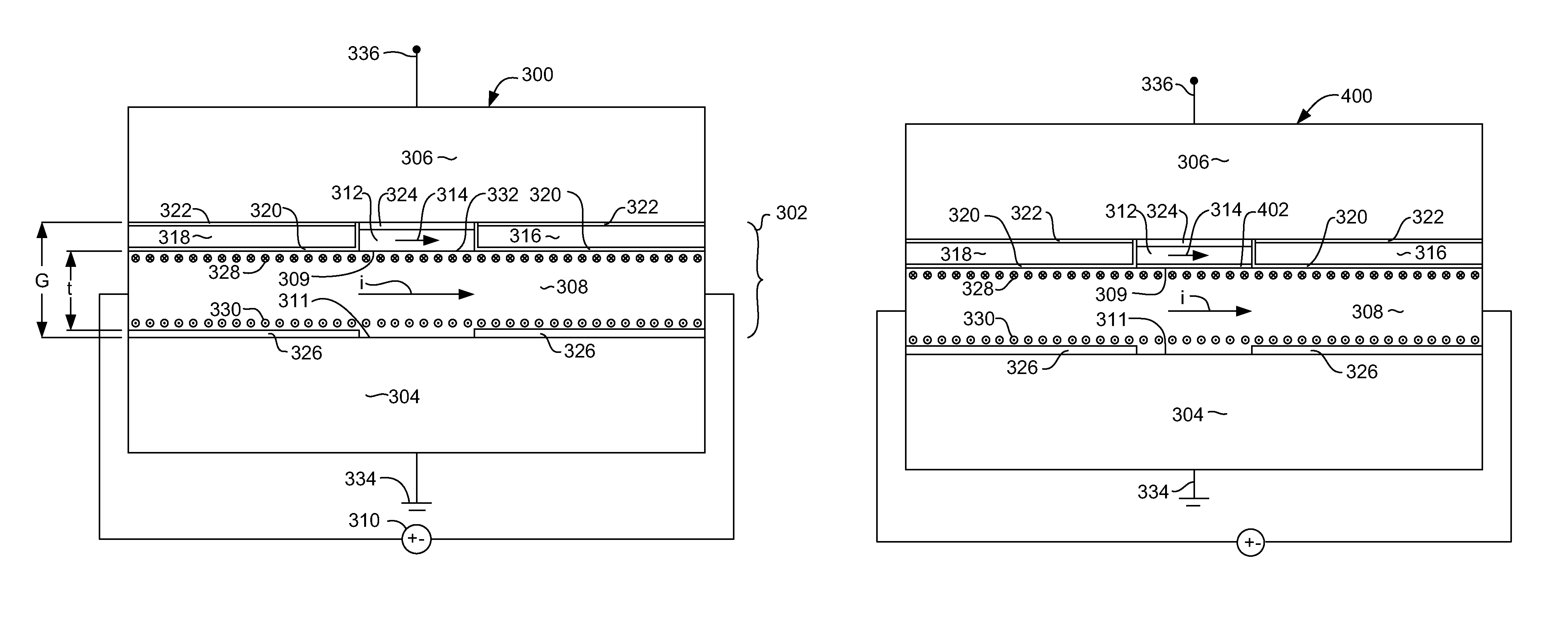
[0021]The following description is of the best embodiments presently contemplated for carrying out this invention. This description is made for the purpose of illustrating the general principles of this invention and is not meant to limit the inventive concepts claimed herein.

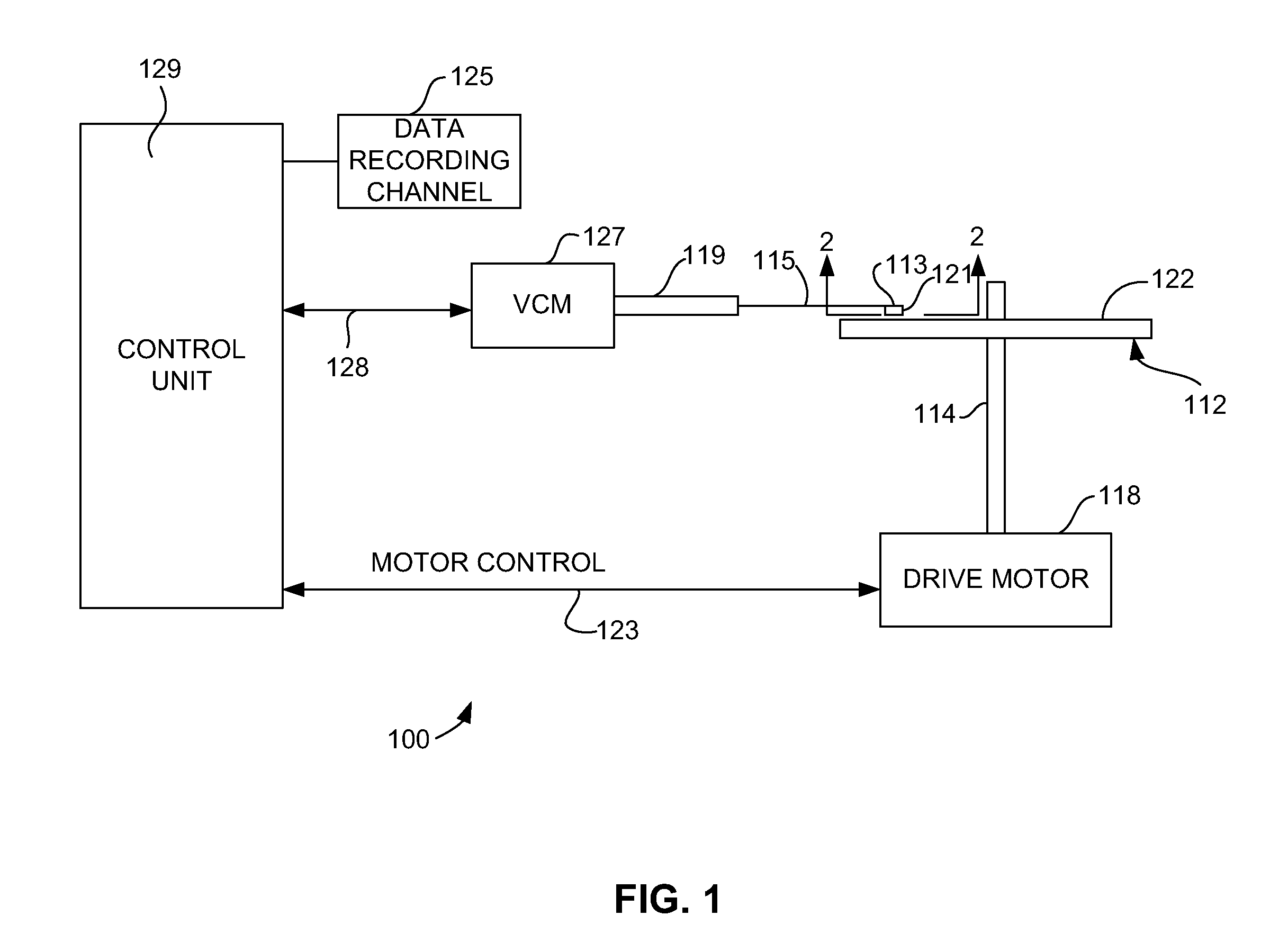
[0022]Referring now to FIG. 1, there is shown a disk drive 100 embodying this invention. As shown in FIG. 1, at least one rotatable magnetic disk 112 is supported on a spindle 114 and rotated by a disk drive motor 118. The magnetic recording on each disk is in the form of annular patterns of concentric data tracks (not shown) on the magnetic disk 112.

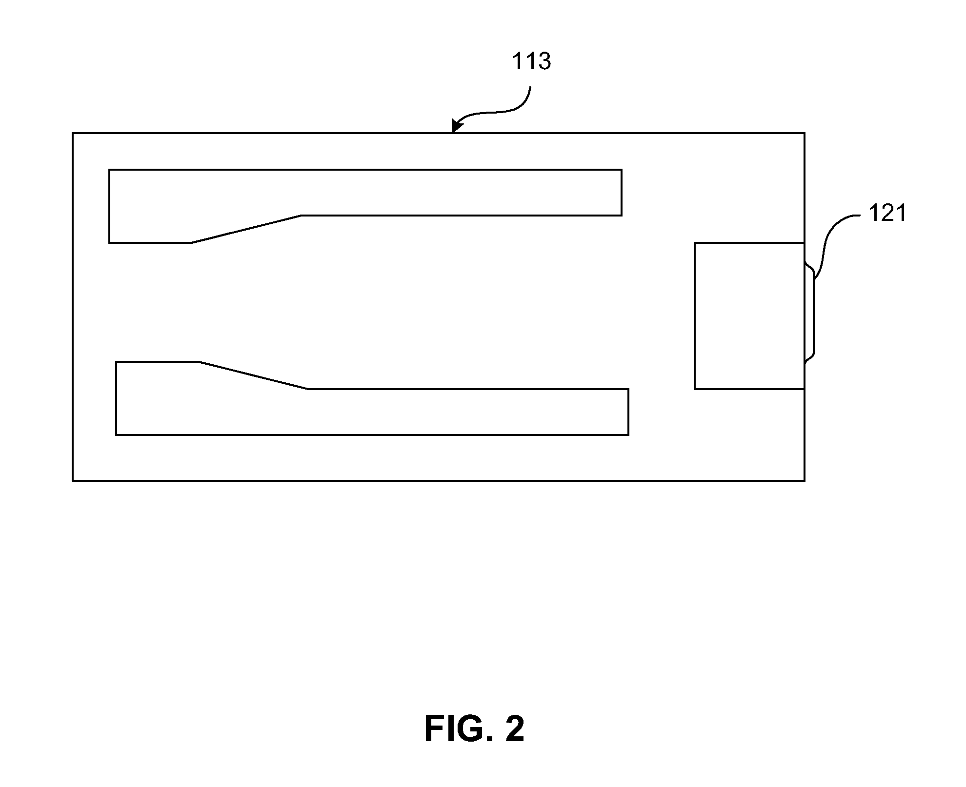
[0023]At least one slider 113 is positioned near the magnetic disk 112, each slider 113 supporting one or more magnetic head assemblies 121. As the magnetic disk rotates, slider 113 moves radially in and out over the disk surface 122 so that the magnetic head assembly 121 can access different tracks of the magnetic disk where desired data are written. Each slider 1...


PUM

PropertyMeasurementUnit
magnetizationaaaaaaaaaa
magnetic fieldaaaaaaaaaa
electrically conductiveaaaaaaaaaa

Abstract

A magnetic sensor utilizing the spin Hall effect to polarize electrons for use in measuring a magnetic field. The sensor eliminates the need for a pinned layer structure or antiferromagnetic layer (AFM layer), thereby reducing gap thickness for increased data density. The sensor includes a non-magnetic, electrically conductive layer that is configured to accumulate electrons predominantly of one spin at a side thereof when a current flows there-through. A magnetic free layer is located adjacent to the side of the non-magnetic, electrically conductive layer. A change in the direction of magnetization in the free layer relative to the orientation of the spin polarized electrons causes a change in voltage output of the sensor.

Description

FIELD OF THE INVENTION[0001]The present invention relates to magnetic data recording and more particularly to a magnetic sensor that utilizes spin Hall effect to provide electron spin polarization.BACKGROUND OF THE INVENTION[0002]At the heart of a computer is an assembly that is referred to as a magnetic disk drive. The magnetic disk drive includes a rotating magnetic disk, write and read heads that are suspended by a suspension arm adjacent to a surface of the rotating magnetic disk and an actuator that swings the suspension arm to place the read and write heads over selected circular tracks on the rotating disk. The read and write heads are directly located on a slider that has an air bearing surface (ABS). The suspension arm biases the slider into contact with the surface of the disk when the disk is not rotating, but when the disk rotates air is swirled by the rotating disk. When the slider rides on the air bearing, the write and read heads are employed for writing magnetic impr...

Claims


Application Information

Patent Timeline
Patent Type & Authority Patents(United States)
IPC IPC(8): G11B5/127G11B5/37H01L43/06G01R33/07G01R33/12
CPCH01L43/06G11B5/374G01R33/07G01R33/1284G11B5/3912H10N52/00
Inventor MIHAJLOVIC, GORANVAN DER HEIJDEN, PETRUS A.
Owner WESTERN DIGITAL TECH INC
Why Eureka
Try Eureka