Defect mending method and structure

A defect repair and defect technology, applied in the field of repair structure, can solve problems such as damage, material oxidation, poor conductivity and adhesion

Inactive Publication Date: 2008-10-01
IND TECH RES INST
View PDF1 Cites 3 Cited by
  • Summary
  • Abstract
  • Description
  • Claims
  • Application Information

AI Technical Summary

Problems solved by technology

In this technology, after the repaired line material is irradiated by laser light, the repair material is easily affected by the energy of the laser light and produces a heat-affected zone phenomenon, so there will be problems of material oxidation and destruction, resulting in poor conductivity and adhesion

Method used


Image

  • Defect mending method and structure
  • Defect mending method and structure
  • Defect mending method and structure

Examples


Embodiment Construction

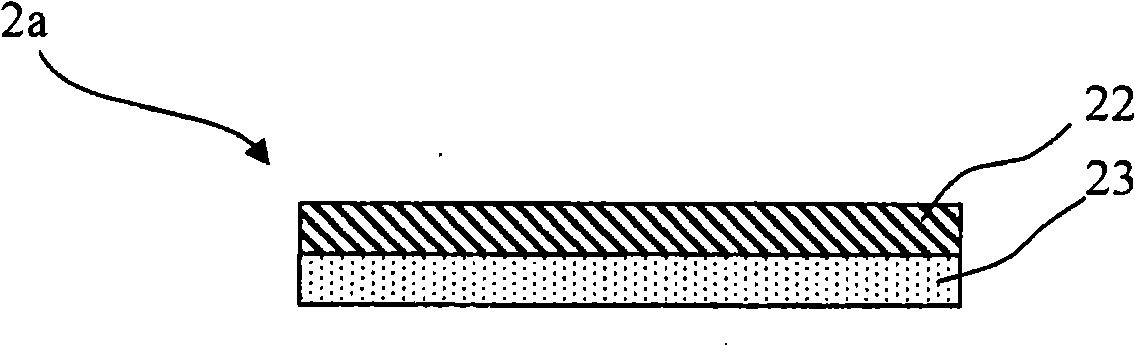
[0112] see Figure 2A As shown, this figure is a schematic diagram of the first embodiment of the defect repairing structure of the present invention. The defect repairing structure 2 a has a conductive adhesive layer 23 , and a repairing material layer 22 is formed on the conductive adhesive layer 23 . The material properties of the conductive adhesive layer 23 are conductive and adhesive, so that the repairing material layer 22 can be easily attached to the defective circuit 21 . The conductive adhesive layer 23 is silver glue in this embodiment. The repairing material layer 22 is a metal material layer, and the metal material can be selected from tungsten, gold, silver, copper, silver glue or molybdenum, but not limited thereto.

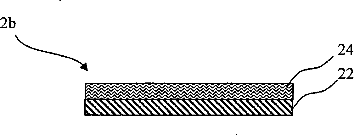
[0113] see Figure 2B As shown, this figure is a schematic diagram of the second embodiment of the defect repairing structure of the present invention. The defect repairing structure 2 b has a repairing material layer 22 , and an intermediate l...


PUM


Abstract

The present invention provides a defect mending structure and a defect mending method. The mending structure has a structure with a plurality of layers to mend the circuit pattern with defect. Besides, the defect mending method provided by the invention mainly uses the impact pressure generated when the transfer material that is has the structure with a plurality of layers receives the irradiation of the electromagnetic wave light source, namely uses the light pressure generated form the impact of the photon and the energy of the electromagnetic wave to generate a molecular bonding breakage or an explosion phenomenon in order to transfer the material to the area to be mended. Through the structure and method provided by the invention, the phenomenon of hot influence caused by the irradiation of the light source on the mending material and the problems of easy oxidization and stress failure caused thereby can be settled.

Description

technical field [0001] The present invention relates to a repairing structure and method, in particular to a repairing circuit with defects by using a multi-layer structure and using the collision pressure generated by the repair base material having a multi-layer structure after being irradiated by an electromagnetic wave light source, so that A defect repairing structure and defect repairing method in which material is transferred to an area to be repaired. Background technique [0002] Flat Panel Display (FPD) is already one of the most important industries in Taiwan, China. With the development of large-size LCD panels and mass production to the seventh-generation factory, the trend of increasing panel size and increasing demand for production capacity and the market Under the demand, the existing repair process faces a huge bottleneck. As shown in Figure 1, the front-end process of flat-panel displays mainly uses photoresist etching technology to form circuit patterns....

Claims


Application Information

Patent Timeline
Patent Type & Authority Applications(China)
IPC IPC(8): G02F1/13B23K26/00
Inventor 廖仕杰陈辉达王仪龙
Owner IND TECH RES INST
Why Eureka
Try Eureka