Electromagnetic wave absorbability plastic foam board

A plastic foam and absorbent technology, applied in the field of electromagnetic wave absorbers, can solve the problems of high cost, unfavorable industrialization development, complicated preparation process, etc., and achieve the effect of light weight, low production cost and easy industrialization

Inactive Publication Date: 2008-10-08
HAINAN UNIVERSITY
View PDF2 Cites 9 Cited by
  • Summary
  • Abstract
  • Description
  • Claims
  • Application Information

AI Technical Summary

Problems solved by technology

[0005] At present, the protection of electromagnetic radiation mainly uses electromagnetic radiation protection materials and products, such as electromagnetic wave absorbing coatings, plates, grease-like materials, etc., among which the electromagnetic wave absorbing plates are made by blending high molecular polymers and electromagnetic wave absorbing agents. into a polymer composite material, as disclosed in the patent application No. 200510060803.7, or mixed with various components and then pressed into shape, such as disclosed in the patent application No. 200410011359.5, etc., the preparation method used The process is relatively complicated and the cost is high, which is not conducive to the development of industrialization

Method used


Image

  • Electromagnetic wave absorbability plastic foam board

Examples


Embodiment 1

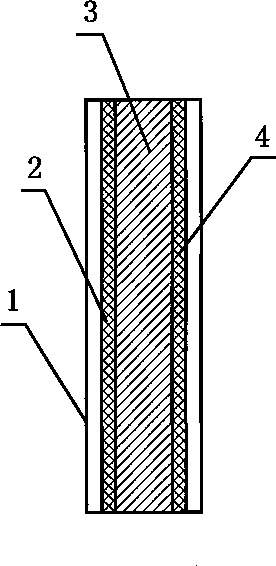
[0019] Use commercially available plastic foam board with a thickness of 20mm. Then on both sides of the board, use adhesive to compound resistive film (area resistance 370Ω□, thickness 0.05mm), conductive film (area resistance 2Ω□, thickness 0.03mm), and then glue on the surface of the resistive film and conductive film. The binding agent pressure composites a protective film, and the protective film is ordinary wall paper (thickness 0.07mm) to obtain a pure density board electromagnetic wave absorber. The absorption effect is 2-5GHz band, the overall absorption is basically above 5dB, and the maximum absorption is 24dB.

Embodiment 2

[0021] Use commercially available plastic foam board with a thickness of 20mm. Then on both sides of the board, use adhesive to compound the resistive film (area resistance 340Ω□, thickness 0.05mm) and conductive film (area resistance 2Ω□, thickness 0.03mm), and then glue on the surface of the resistance film and the conductive film. The binding agent pressure composites a protective film, and the protective film is ordinary wall paper (thickness 0.07mm) to obtain a pure density board electromagnetic wave absorber. The absorption effect is 2-5GHz band, the overall absorption is basically above 5dB, and the maximum absorption is 20dB.

Embodiment 3

[0023] Use commercially available plastic foam board with a thickness of 20mm. Then on both sides of the board, use adhesive to compound resistive film (area resistance 430Ω□, thickness 0.05mm) and conductive film (area resistance 2Ω□, thickness 0.03mm), and then glue on the surface of the resistive film and conductive film. The binding agent pressure composites a protective film, and the protective film is ordinary wall paper (thickness 0.07mm) to obtain a pure density board electromagnetic wave absorber. The absorption effect is in the 2-5GHz frequency band, the overall absorption is basically above 5dB, and the maximum absorption is 22dB.


PUM

PropertyMeasurementUnit
electrical resistanceaaaaaaaaaa
thicknessaaaaaaaaaa

Abstract

The invention discloses an electromagnetic wave absorbent plastic foam board, wherein two lateral surfaces of a dielectric body [3] have a resistive film [2] and a conductive film [4] bonded by a bonder. A layer of protective film [1] is further bonded on the outsides of the resistive film and the conductive film through pressure by the bonder. The invention with low manufacturing cost is simply structured, provided with advantages of radiation absorption, environment protection, light weight, easy industrialization etc, which can be widely applied to the electromagnetic radiation protective clapboard of computer room, the electromagnetic radiation protection of office and residence, anti-electromagnetic interference, radiation protection and information leakage protection in bank and hospital etc.

Description

Technical field [0001] The invention relates to an electromagnetic wave absorber, in particular to an electromagnetic wave absorbing plastic foam board. Background technique [0002] With the rapid development of the information society, electronic products are becoming more and more popular. While bringing great convenience to people, electronic products also bring certain harm. In particular, the immense popularity of electronic equipment with built-in information processing devices and the increasing speed of CPU operations have resulted in high-frequency electromagnetic radiation and noise pollution becoming more and more serious. The deteriorating electromagnetic environment not only affects the signal propagation of communications, computers, and various electronic systems on which human life is increasingly dependent, causes system devices to malfunction, and brings unpredictable disasters, but also threatens human health. Studies have shown that working, studying and livi...

Claims


Application Information

Patent Timeline
Patent Type & Authority Applications(China)
IPC IPC(8): H05K9/00B32B7/12B32B5/18
Inventor 郝万军张月芳赵小亮陈健健
Owner HAINAN UNIVERSITY
Why Eureka
Try Eureka