Method for transferring and device for handling electronic components

A technology of electronic components and transmission components, applied in the direction of electrical components, electrical components, circuits, etc., can solve problems such as speed reduction and complex mechanical structures, and achieve the effects of improving reliability, increasing processing speed, and simplifying further processing

Inactive Publication Date: 2008-10-08
西门子电子装配系统两合公司
View PDF2 Cites 7 Cited by
  • Summary
  • Abstract
  • Description
  • Claims
  • Application Information

AI Technical Summary

Problems solved by technology

But this inverting device has the same disadvantage as the flip-chip manipulator described above, that is, it needs a complex mechanical structure, which makes the speed of the whole assembly process greatly reduced

Method used


Image

  • Method for transferring and device for handling electronic components
  • Method for transferring and device for handling electronic components
  • Method for transferring and device for handling electronic components

Examples


Embodiment Construction

[0035] It should be noted here that the only difference in the reference symbols of the same elements or corresponding elements in the various drawings lies in the first number and / or the letter appended thereto.

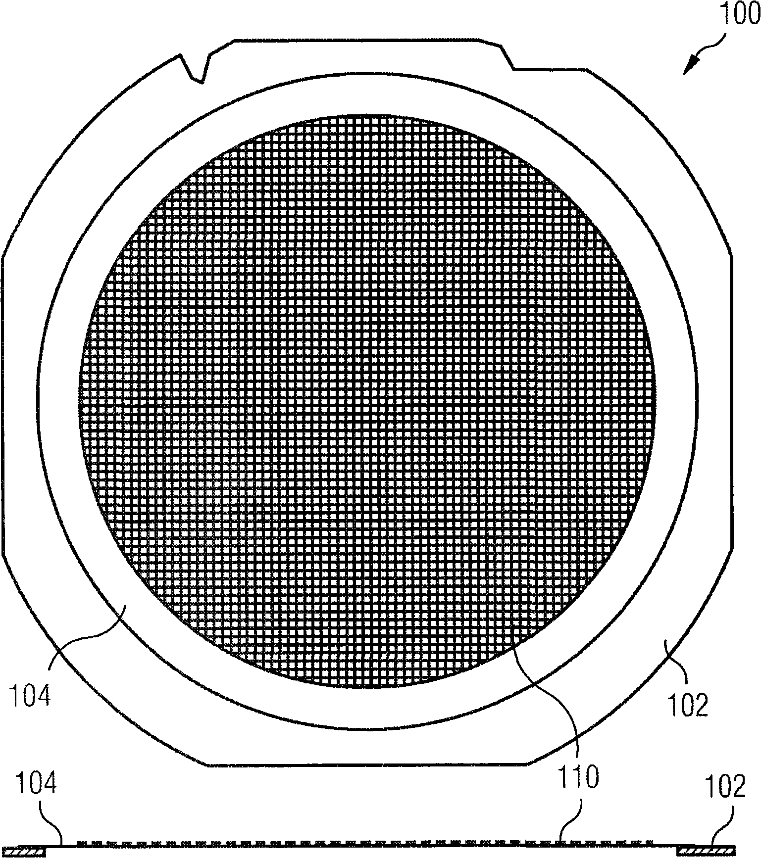
[0036] figure 1 The wafer holding device 100 shown has a ring clamp 102 to which a carrier film 104 is fastened. An entire wafer system consisting of a plurality of electronic components 110 is fixed on the carrier film 104 by means of adhesive forces. Electronic components 110 without housings are arranged on the adhesive carrier film 104 in the form of a mesh. The way to load the component 110 on the wafer holding device 100 is to first glue the entire disk-shaped wafer on the carrier film 104 . The way to divide the wafer into a plurality of electronic components 110 is to saw the wafer along the intersection lines perpendicular to each other with a precision sawing tool, or to divide the wafer through a precise etching process. The connection contacts of the ...


PUM


Abstract

The invention relates to a method for transferring electronic components (210), especially flip-chips or bare dies, from a sticky support film (204) onto a transfer head (250). The inventive method comprises the following steps: a) transferring the support film (204) to a vacuum pick-up device (220) which comprises a planar suction surface (223) which is provided with openings, a face of the support film (204) carrying the components (210) facing the suction surface, b) applying a reduced pressure to the vacuum pick-up device (220) so that the components (210) are sucked off by the suction surface, c) reducing the stickiness of the support film (204) so that the adhesive force exerted by the support film (204) on the components (210) is smaller than the suction force exerted by the vacuum pick-up device (220) on the components (210), d) removing the support film (204); from the vacuum pick-up device (220), the components (210) remaining on the vacuum pick-up device (220), and e) picking up the components (210) by means of a transfer head (250) which comprises at least one component holding device (252). The invention also relates a device for handling electronic components (210), especially for use as a vacuum pick-up device (220) for carrying out the inventive method.

Description

technical field [0001] The invention relates to a method for transferring electronic components from an adhesive carrier film, on which usually all components of an entire wafer are fixed, to a transfer head, whereby the transferred components can be mounted to an electronic circuit substrate superior. The invention also relates to a device for handling electronic components, said device being used in particular as a vacuum pick-up device during the implementation of the method described above. Background technique [0002] In view of the increasing miniaturization of electronic components, in the near future, in order to achieve the purpose of more stable delivery of components in the assembly process, the electronic components that need to be mounted on the electronic circuit substrate will be repackaged. Cost advantage. This option of loading components onto dedicated component conveyors is often used when components are conveyed individually for the assembly process. ...

Claims


Application Information

Patent Timeline
Patent Type & Authority Applications(China)
IPC IPC(8): H05K13/04H05K13/02H01L21/00
CPCH01L21/67132H01L21/67005
Inventor 冈特·希贝尔
Owner 西门子电子装配系统两合公司
Why Eureka
Try Eureka