Liquid crystal display panel and its substrate preparation method

A liquid crystal display panel and substrate technology, applied in nonlinear optics, instruments, optics, etc., can solve the problems of lowering the display quality and practicability of liquid crystal display panels, gray spots, residual pollution sources, etc.

Inactive Publication Date: 2008-10-22
INNOLUX CORP
View PDF0 Cites 72 Cited by
  • Summary
  • Abstract
  • Description
  • Claims
  • Application Information

AI Technical Summary

Problems solved by technology

[0006] However, when the alignment roller rolls over the alignment film, there will be pollution sources remaining on the alignment film in the display area of ​​the upper and lower substrates, such as the resin coated on the surface of the hair of the alignment roller, the polyimide on the hair , dust or foreign matter
Therefore, display defects, such as clusters of gray spots or bright spots, will occur in the subsequently completed liquid crystal display panel.
As a result, the display quality and practicality of the LCD panel will be greatly reduced.

Method used


Image

  • Liquid crystal display panel and its substrate preparation method
  • Liquid crystal display panel and its substrate preparation method
  • Liquid crystal display panel and its substrate preparation method

Examples


Embodiment 1

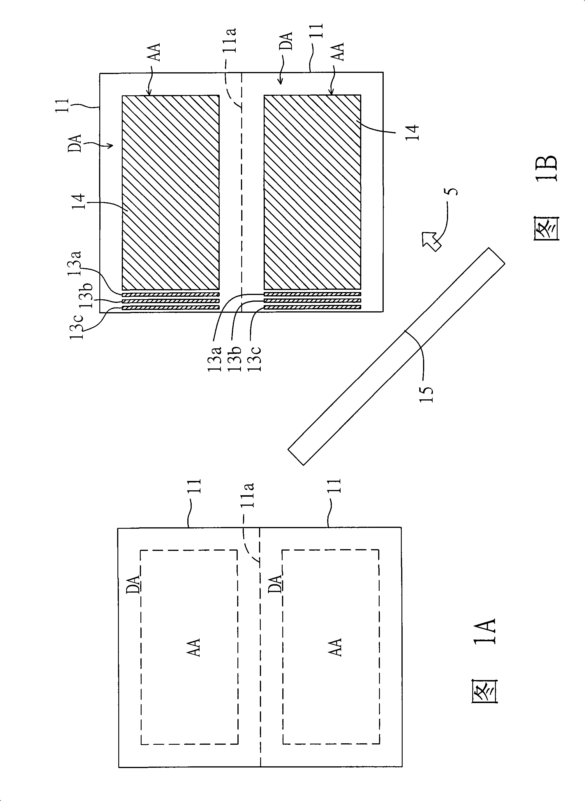
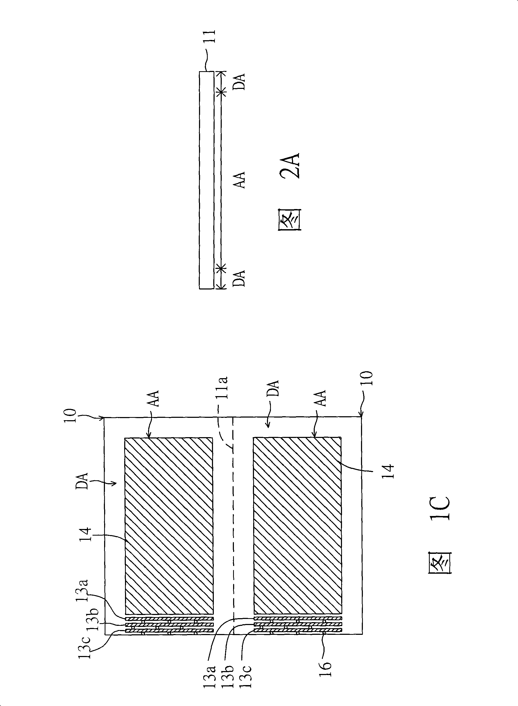
[0020] Please refer to FIG. 1A to FIG. 2C at the same time. FIG. 1A to FIG. 1B are top views of the manufacturing process of the substrate of the liquid crystal display panel according to Embodiment 1 of the present invention, and FIG. 2A to FIG. Process cross-section of the substrate. First, referring to FIG. 1A and FIG. 2A , a substrate 11 is provided, and a display area AA and a surrounding non-display area DA are defined on the substrate 11 . Wherein, the display area AA corresponds to the pixel array area and the liquid crystal filling area of ​​the liquid crystal display panel, and the surrounding non-display area DA corresponds to the external circuit connection area of ​​the liquid crystal display panel. In addition, it is possible to divide, for example, two small-area substrates 11 in a large-area substrate, and define a cutting line 11 a between the two substrates 11 .

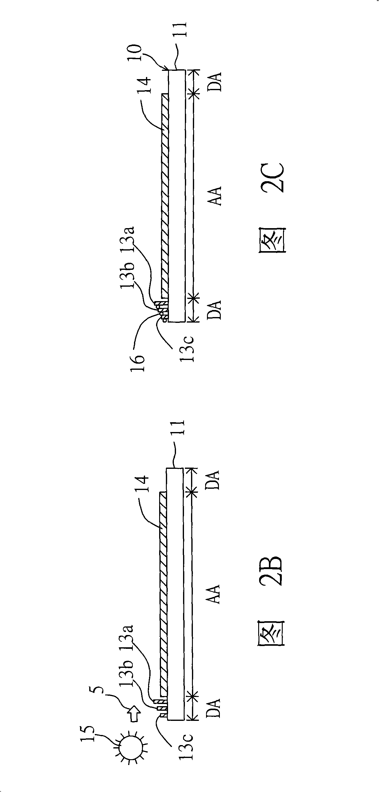
[0021] Next, as shown in FIG. 1B and FIG. 2B, an alignment film 14 and several barrier walls ar...

Embodiment 2

[0027] Please refer to FIG. 3 , which is a top view of a substrate of a liquid crystal display panel according to Embodiment 2 of the present invention. The difference between the substrate 20 of the liquid crystal display panel of the present embodiment and the substrate 10 of the liquid crystal display panel of the first embodiment lies in the barrier walls 23 a - 23 c , and the rest of the same constituent elements continue to use reference numerals and will not be repeated.

[0028] As shown in FIG. 3, the retaining walls 23a-23c are discontinuously arranged in the surrounding non-display area DA, and located outside the central non-display area AA, and have almost the same height or different heights to form heights. segment difference. The blocking wall 23a is closest to the display area AA, while the blocking wall 23c is farthest from the display area AA. The heights of the retaining walls 23a-23c gradually increase from the edge of the substrate 11 to the edge of the ...

Embodiment 3

[0030] Please refer to FIG. 4 , which is a top view of a substrate of a liquid crystal display panel according to Embodiment 3 of the present invention. The difference between the substrate 30 of the liquid crystal display panel of this embodiment and the substrate 10 of the liquid crystal display panel of the first embodiment lies in the barrier walls 33 a - 33 c. The rest of the same constituent elements continue to use the labels and will not be repeated.

[0031] As shown in FIG. 4 , the retaining walls 33 a - 33 c are continuously disposed in the peripheral non-display area DA and surround the central non-display area AA, and have almost the same height or different heights to form height differences. The blocking wall 33a is closest to the display area AA, while the blocking wall 33c is farthest from the display area AA. Wherein, the blocking walls 33 a - 33 c are used to block pollution sources from the display area AA after the rubbing alignment of the alignment film 14...


PUM


Abstract

The invention discloses a liquid crystal display panel, comprising a first substrate, a second substrate and a liquid crystal layer, wherein, the liquid crystal layer is arranged between the first substrate and the second substrate; the first substrate comprises a bottom material, an alignment film and a plurality of retaining walls; the bottom material is defined with a display area and a surrounding non-display area, the alignment film is arranged in the display area; the plurality of retaining walls are arranged in the surrounding non-display area; moreover, the heights of the plurality of retaining walls are greater than the height of the alignment film; a pollution source is blocked outside of the display area by the retaining walls after the friction alignment action of the alignment film, thereby preventing the pollution source from falling into the display area and avoiding the display detects such as group gray spots or light spots of the liquid crystal display panel. Therefore, the display quality and the practicability of the liquid crystal display panel are greatly improved.

Description

technical field [0001] The present invention relates to a method of manufacturing a liquid crystal display panel and its substrate, and in particular to a method of manufacturing a liquid crystal display panel and its substrate that prevents pollution sources from the display area after the rubbing alignment of the alignment film . Background technique [0002] With the development of flat panel displays, liquid crystal display panels have been widely used in various aspects of daily life, such as televisions, monitors, computer screens, notebook computers, personal digital assistants, mobile phones and other electronic products. [0003] The alignment film (alignment film) is a main component of the liquid crystal display panel, and its function is to make the liquid crystal molecules in the liquid crystal display panel and the surface of the alignment film tilt at a certain angle (ie, pretilt angle, pretilt angle) to achieve liquid crystal display. The effect of uniform m...

Claims


Application Information

Patent Timeline
Patent Type & Authority Applications(China)
IPC IPC(8): G02F1/1333G02F1/1339G02F1/1337G02F1/1362
Inventor 高克毅侯志昌杨坤璋林吉宏
Owner INNOLUX CORP
Why Eureka
Try Eureka