Semiconductor quantum well photon detecting element

A photon detector, photon detection technology, applied in semiconductor devices, electrical components, circuits, etc., can solve problems such as inability, difficulty in matching the semiconductor characteristic frequency and surface plasmon mode, and wide-ranging adjustment

Inactive Publication Date: 2008-11-05
FUDAN UNIV
View PDF2 Cites 10 Cited by
  • Summary
  • Abstract
  • Description
  • Claims
  • Application Information

AI Technical Summary

Problems solved by technology

However, the above-mentioned disclosed technology has difficulties in tuning the matching degree of the semiconductor characteristic frequency and the surface plasmon mode, because the dielectric properties and band gap of the semiconductor are the unique properties of the materia

Method used


Image

  • Semiconductor quantum well photon detecting element
  • Semiconductor quantum well photon detecting element
  • Semiconductor quantum well photon detecting element

Examples


Embodiment 1

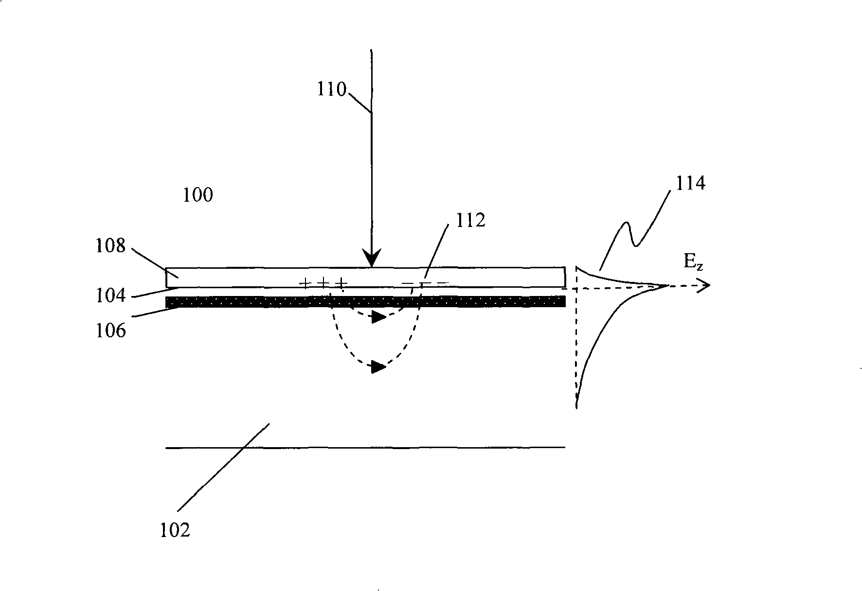
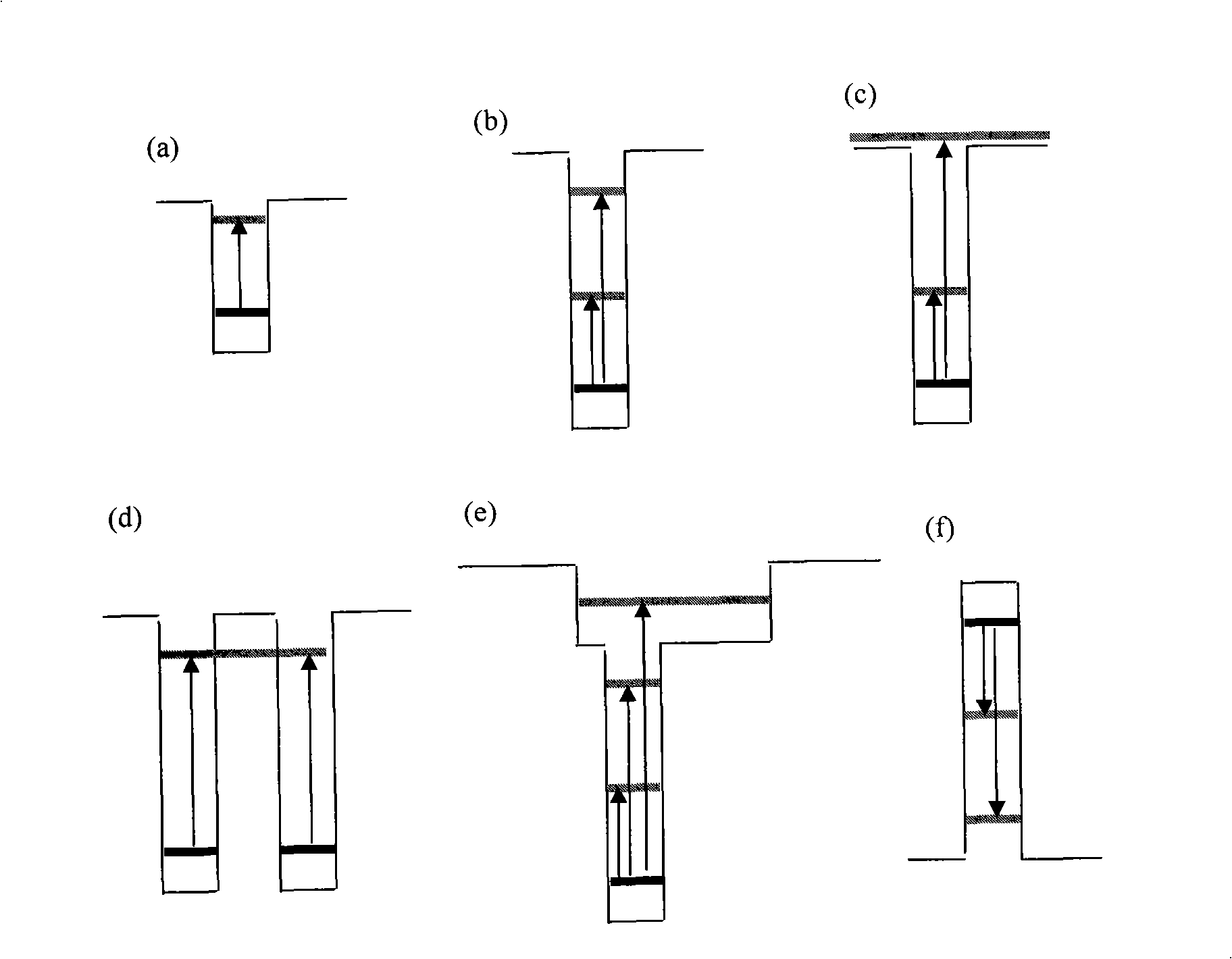
[0039] like figure 1 As shown, the quantum well photon detection device 100 includes: a semiconductor GaAs layer 102, which has an InGaAs / GaAs quantum well layer 106 near the surface 104 on one side of the semiconductor layer 102; and a metal Au sub-wavelength period on the semiconductor surface 104 Sexual Structures 108, see Figure 4 a. The incident light wave 110 is incident from the direction perpendicular to the semiconductor surface 104 and the quantum well layer 106 and is finally absorbed by the quantum well layer 106, generating a surface plasmon wave 102, whose vertical direction electric field component E z As shown in 114. E. z Excite subband transitions in quantum wells (see image 3 a) The energy is absorbed by the quantum well to complete the photon detection process.

Embodiment 2

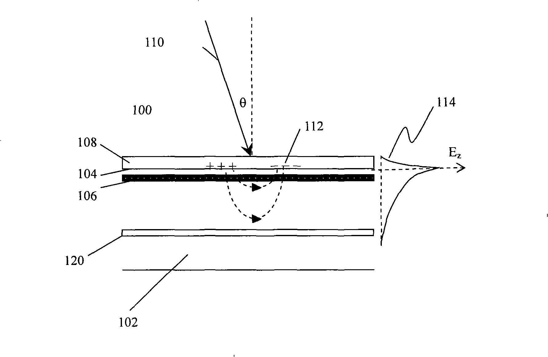
[0041] like figure 2 shown in figure 1 A heavily doped Si layer or Bragg mirror layer 120 is introduced on the basis of the structure. The incident light wave 110 is incident at an angle θ away from the normal direction. Also in the metallic Au subwavelength periodic structure ( Figure 4 b) The surface plasmon wave is excited, and its energy is partially absorbed by the quantum well layer; the transmitted part is reflected by the heavily doped layer or the Bragg reflection layer and then again the quantum well layer, so that the energy is absorbed by the quantum well layer with high efficiency .

Embodiment 3

[0043] like Figure 6 shown, using Figure 5 In the metal microhole array structure, the period is 4.5 microns, the side length of the microholes is about 2 microns, the material is Au, and the thickness is 100 nanometers. The detector structure is formed on the quantum well material ( Figure 6 a). The quantum well material structure includes: GaAs substrate layer, epitaxial buffer layer, double quantum well layer (the thickness of the upper quantum well layer is 10 nanometers, which is the photodetection layer; the lower layer is 50 nanometers, which is the channel layer; the double quantum well layer uses a graded composition Barrier layer), AlGaAs barrier layer and appropriate doping, GaAs cap layer. Then through a certain process technology to form Figure 6 In the device structure shown in (a), AuGeNi is used as the source and drain contact material to form an ohmic contact through proper processing. The metal microhole array structure 108 is coupled with the quantu...


PUM

PropertyMeasurementUnit
Thicknessaaaaaaaaaa
Thicknessaaaaaaaaaa

Abstract

The invention belongs to the technical field of the photodetection, particularly to a semiconductor quantum well photon detector, which includes a semiconductor layer, and a quantum well layer is arranged near the surface of one side of the semiconductor, wherein the quantum well is provided with certain carrier density and at least two energy levels; a metal layer with the sub-wavelength hole periodic structure, arranged on the surface of one side of the semiconductor; an incident light wave, on the direction vertical to the one side surface of the semiconductor and the quantum well layer, incident from the front of the metal layer or the other surface of the semiconductor layer, and finally adsorbed by the quantum well layer. The invention performs the optical couple by using the metal sub-wavelength periodic structure, realizes the active absorption of the quantum well structure to the vertical incident light, meanwhile the semiconductor energy gap technology is combined with the surface of the metal periodic structure, which realizes the convenient tune of the coupling way and the semiconductor quantum well light wave detection in the wide wavelength range.

Description

technical field [0001] The invention belongs to the technical field of light wave detection, and in particular relates to a semiconductor quantum well detection device. Background technique [0002] Devices using quantum well structures are one of the main technologies for light wave detection, especially for light wave detection in the mid- and far-infrared bands. However, the light wave absorption of the semiconductor quantum well structure is limited by the "polarization selection law" widely known in the field, that is, the quantum well structure can only absorb light waves with non-zero electric field components perpendicular to the quantum well plane, and for practical applications In most cases, the absorption of vertically incident light waves is extremely small, for example, refer to Document 1. Therefore, in actual device applications, it must be combined with complex processes such as side-tilt incidence (such as document 2), grating coupling (such as document 5)...

Claims


Application Information

Patent Timeline
IPC IPC(8): H01L31/111
CPCH01L31/035209H01L31/02327H01L31/112
Inventor 安正华周磊陈张海沈学础
Owner FUDAN UNIV
Why Eureka
Try Eureka