Method of manufacturing a semiconductor device

A semiconductor and device technology, applied in the field of manufacturing semiconductor devices, can solve problems such as reliability, reduce injection damage, and facilitate in-depth access

Active Publication Date: 2008-11-05
AMPLEON NETHERLANDS
View PDF2 Cites 14 Cited by
  • Summary
  • Abstract
  • Description
  • Claims
  • Application Information

AI Technical Summary

Problems solved by technology

Additionally, implant damage due to high-energy ions creates reliability issues

Method used


Image

  • Method of manufacturing a semiconductor device
  • Method of manufacturing a semiconductor device
  • Method of manufacturing a semiconductor device

Examples


Embodiment Construction

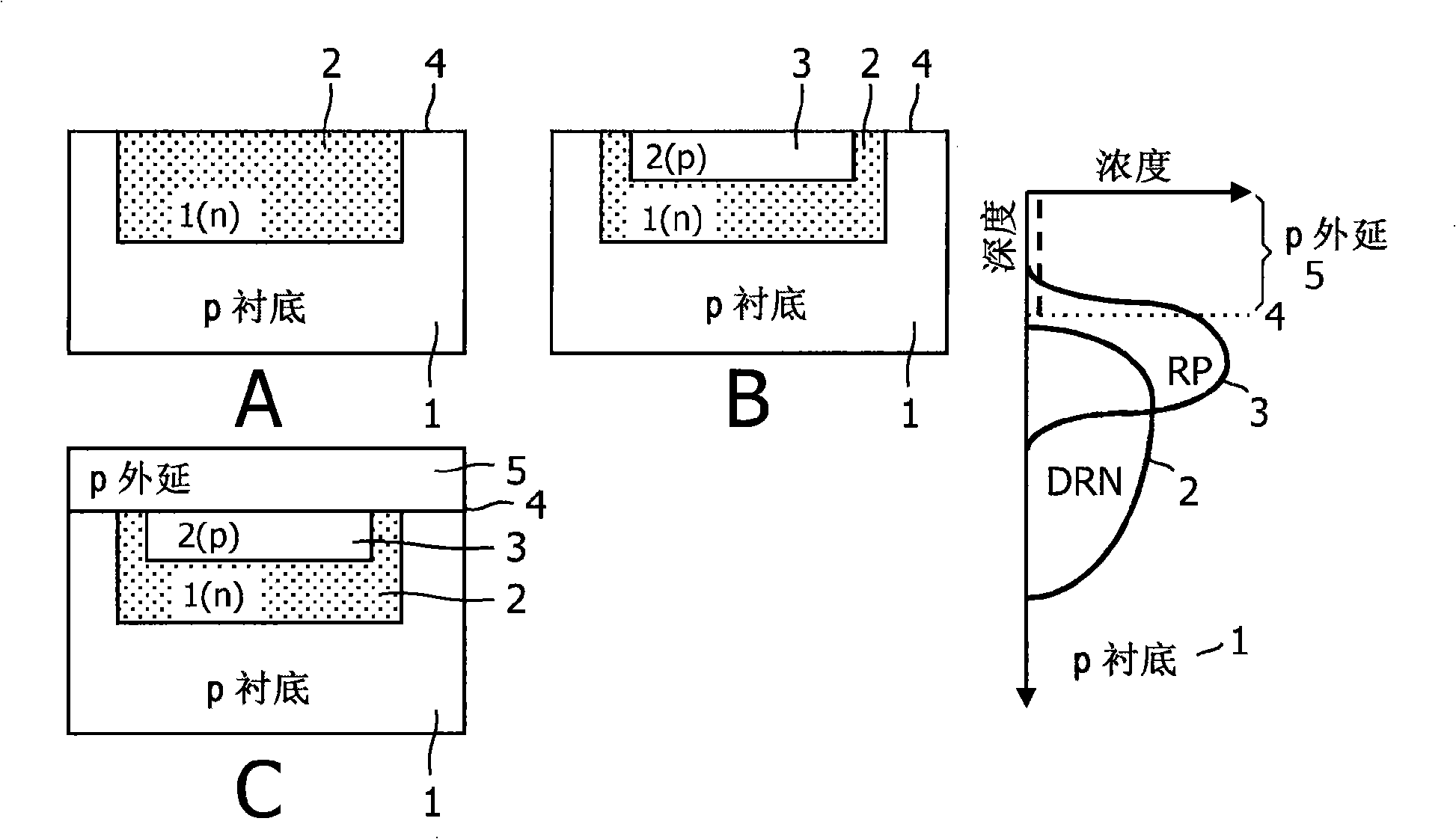
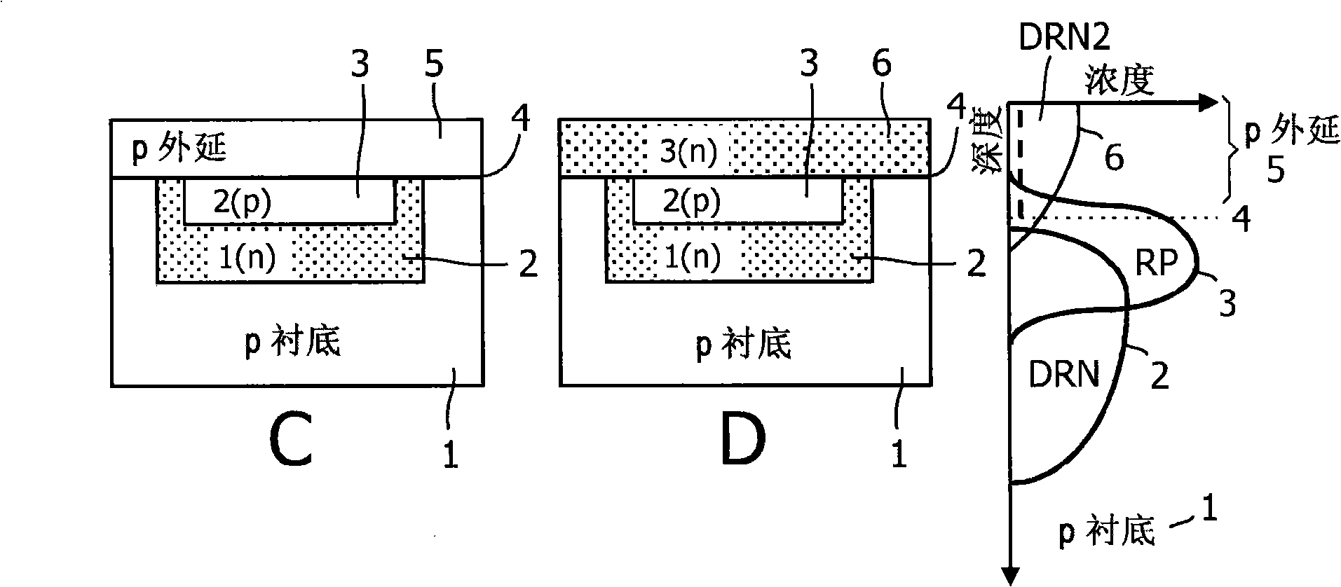
[0039] Figure 1 shows a first preferred embodiment of the method according to the invention. A p-type Si substrate 1 is implanted with an n-type dopant atom mask to form a first region 2 . In this example, P atoms are used with an implant energy of 100keV and a dose of approximately 6×10 16 at / cm 2 . For RESURF, the implant dose is preferably at 1×10 12 and 1×10 13 at / cm 2 range between. A high temperature diffusion step of 540 minutes at 1150° C. allows the n-type dopant atoms to penetrate deeper into the substrate, thereby forming a deep n-type region 2 (labeled here Deep Resurf n, DRN, see FIG. 1A ).

[0040] The second region 3 is formed by implanting a p-type dopant, such as boron or indium, using a mask, on the surface 4 ( FIG. 1B ) of the substrate 1 . Here, boron is implanted at an energy of 100-180keV, and its dose is about 6×10 12 at / cm 2 . For Resurf, the injection dose is preferably at 1×10 12 and 1×10 13 at / cm 2 range between. Therefore, a p-type lay...


PUM


Abstract

The method of the invention discloses a cheaper way of manufacturing a semiconductor device such as a lateral high voltage field-effect (HV-FET) transistor. The method comprises: a substrate of a first conductivity type (1) , - Implanting a first dopant to form a first region (2) of a second conductivity type in the substrate, (and diffusing this) - Forming a second region (3) of the first conductivity type, the first region (2) and the second region (3) forming a pn junction. The second region (3) is a surface layer which is formed by implanting the second dopant at the surface (4) of the substrate. - Subsequently the surface layer is covered by forming a first epitaxial layer (5) of the first conductivity type on the surface layer (3) . The use of an expensive high energy implanter (MeV) can be omitted in the manufacturing of one or more regions disposed on top of each other, thereby obtaining a reduction in cost .

Description

technical field [0001] The present invention relates to a method of manufacturing a semiconductor device, comprising: [0002] - a substrate with a surface of the first conductivity type, [0003] a) implanting the first dopant, thereby forming a first region of the second conductivity type in the substrate, [0004] b) implanting a second dopant into the first region, thereby forming a second region of the first conductivity type, and forming a pn junction between the first region and the second region. Background technique [0005] In US 4,754,310 ( Image 6 , 7) shows a lateral HV-FET with multiple alternating p-n layers in the drift region. High voltage FETs are fabricated using multiple epitaxial layers of alternating conductivity types. The interleaved structure of first and second regions of alternating conductivity type forms a drift region within the high voltage transistor, which carries the high voltage present in the depleted drift region. In this way, multip...

Claims


Application Information

Patent Timeline
Patent Type & Authority Applications(China)
IPC IPC(8): H01L29/06
CPCH01L29/0634H01L29/0873H01L29/0878H01L29/0886H01L29/1083H01L29/1095H01L29/42368H01L29/66681H01L29/7816
Inventor 阿德里安努斯·W·卢迪克休斯伊内兹·M·魏兰琼·维夏德·斯特里耶克
Owner AMPLEON NETHERLANDS
Why Eureka
Try Eureka