Liquid crystal display panel and its array substrate

A technology of liquid crystal display panels and array substrates, applied in nonlinear optics, instruments, optics, etc., which can solve the problems of glued liquid crystal injection port frame, limited pen closing form, missing corners and damage, missing corners and fragments, etc. Achieve the effect of avoiding bad cutting

Inactive Publication Date: 2008-11-19
AU OPTRONICS CORP
View PDF0 Cites 16 Cited by
  • Summary
  • Abstract
  • Description
  • Claims
  • Application Information

AI Technical Summary

Problems solved by technology

[0004] Because it is not easy to control the amount of glue sprayed at the opening and closing positions of the coating of the frame glue 108 of the liquid crystal injection port 110, after the thin film transistor array substrate 102 and the color filter array substrate 104 are assembled, it is easy to have the frame glue 108 at the opening and closing position. The position of the pen shows an enlarged area of ​​overflowing glue
If the excess glue exceeds the cutting line of the motherboard (such as one side 112 of the liquid crystal display panel 100), it will make cutting difficult, and even cause chipping and damage
[0005] In order to avoid the disadvantages of difficult cutting, missing corners, and fragments caused by the above-mentioned overflowing glue, the general existing solution is to increase the distance between the starting and closing positions of the frame glue 108 and the edge 112 as the panel cutting line. , but this method tends to have the following disadvantages and limitations:
[0006] 1. Compress the space of other manufacturing processes, so that the printing area of ​​the alignment film (PI) becomes smaller, which greatly increases the probability of poor printing of PI
[0007] 2. The opening and closing form of the liquid crystal injection port frame glue is limited: Generally, the distance between the starting and closing position and the cutting line has reached the lower limit of the design, and the frame glue can only be applied in a flattened way, which will not be able to In response to the requirements of the latter stage, other designs are made to improve the problems related to liquid crystal injection
[0008] 3. Under the requirement of the narrower frame of the product, the smaller the visible area of ​​the product is from the boundary (that is, the cutting line), so the distance between the starting and closing positions of the frame glue and the cutting line cannot be effectively shortened, so the existing technology The practice is not applicable to products with narrow frame

Method used


Image

  • Liquid crystal display panel and its array substrate
  • Liquid crystal display panel and its array substrate
  • Liquid crystal display panel and its array substrate

Examples


Embodiment Construction

[0052] The making and using of the presently preferred embodiments described are discussed in detail below. It should be appreciated, however, that the present invention provides many applicable inventive concepts, which can be embodied in a wide variety of specific situations. The specific examples discussed are merely illustrative of specific ways to make and use the described invention, and do not limit the scope of the invention.

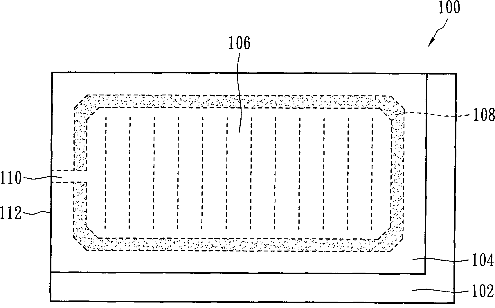
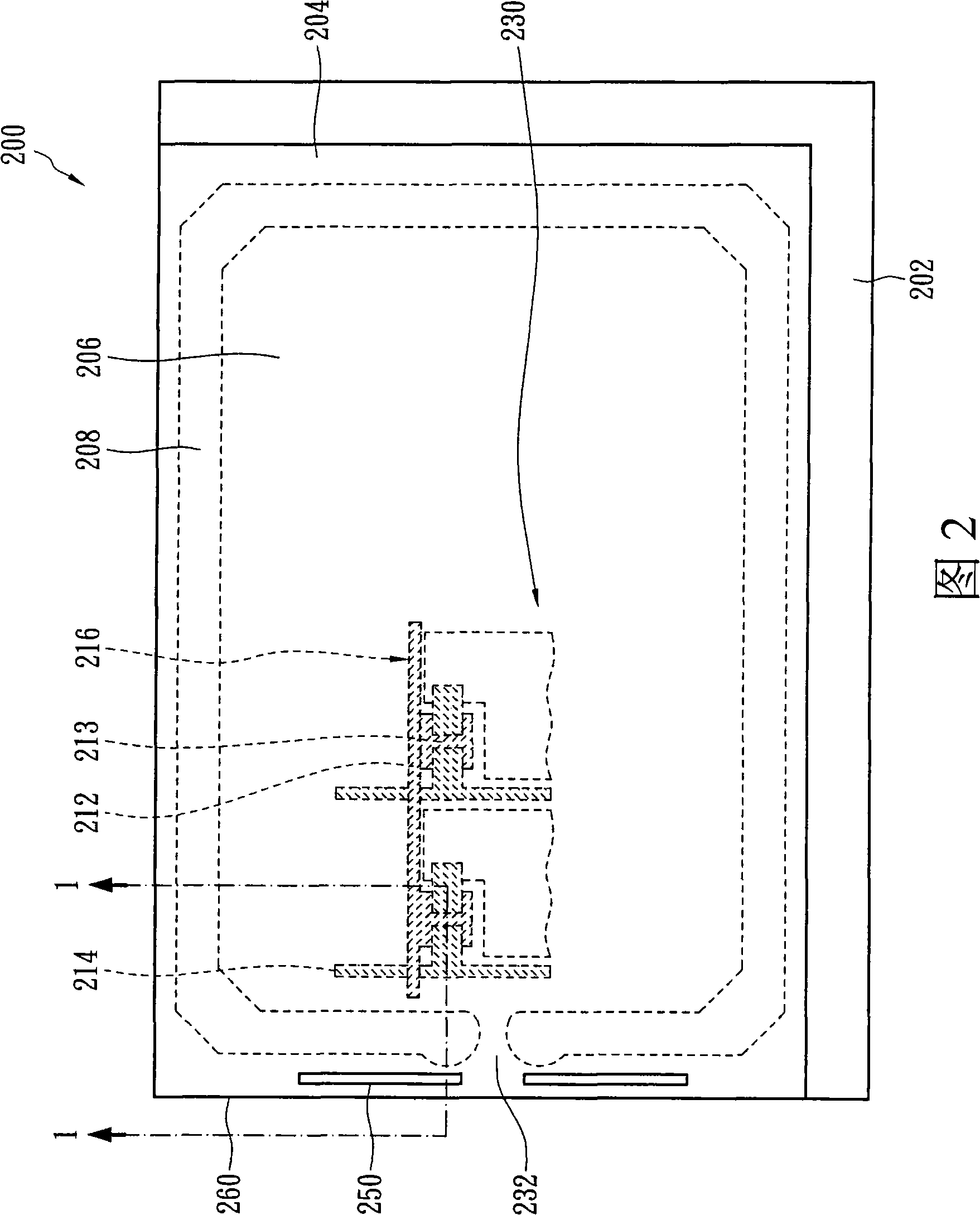
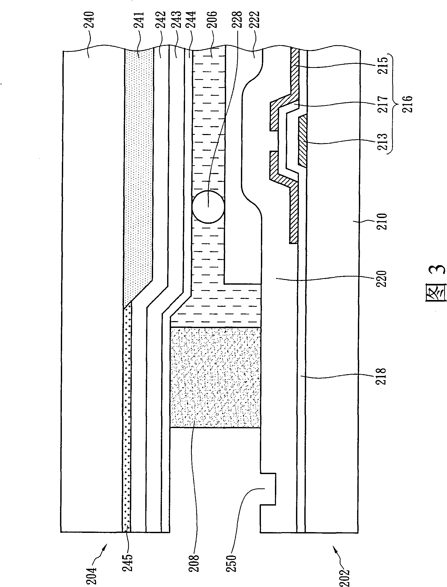
[0053] FIG. 2 shows a liquid crystal display panel 200 according to an embodiment of the present invention, and FIG. 3 is a schematic cross-sectional view of the first embodiment along the line 1-1 in FIG. 2 . The liquid crystal display panel 200 mainly includes a thin film transistor array substrate 202 , a color filter array substrate 204 , a sealant 208 , and a liquid crystal layer 206 injected into the space formed by the aforementioned three through a liquid crystal injection port 232 .

[0054] The thin film transistor array substrate 202...


PUM

PropertyMeasurementUnit
thicknessaaaaaaaaaa

Abstract

The invention relates to a liquid crystal display panel and an array substrate of the liquid crystal display panel; the liquid crystal display panel comprises an array substrate, an opposite substrate and a liquid crystal layer. The opposite substrate and the array substrate are oppositely arranged; the liquid crystal layer is arranged between the array substrate and the opposite substrate. In one embodiment, the array substrate comprises a substrate, an array, a frame adhesive and an adhesive cutting structure. The array can be a thin-film transistor array or a color filter array, which is arranged on the substrate. The frame adhesive has a first end and a second end; the first end and the second end form a liquid crystal injection opening. The adhesive cutting structure is arranged on the substrate, at least between the first end of the frame adhesive and one side of the substrate. The invention can prevent the possibly over-spilled frame adhesive from extending to the side of the substrate when the array substrate and the opposite substrate are erected, so as to avoid bad cutting.

Description

technical field [0001] The invention relates to a liquid crystal display panel and an array substrate thereof, in particular to a liquid crystal display panel and an array substrate thereof with a glue-stopping structure of a liquid crystal injection port. Background technique [0002] Liquid crystal displays (LCDs) have been widely used in today's display applications due to their advantages of thinness, light weight, low power consumption, and low radiation. The liquid crystal display mainly includes a liquid crystal panel and a backlight module. The backlight module is used to provide a light source for the liquid crystal panel, and an electric signal is used to control the direction of liquid crystal molecules of the liquid crystal panel to display images. [0003] figure 1 It is a top perspective view of a liquid crystal display panel 100 , wherein a color filter (Color Filter; CF) array substrate 104 is disposed above a thin film transistor (Thin Film Transistor; TFT)...

Claims


Application Information

Patent Timeline
Patent Type & Authority Applications(China)
IPC IPC(8): G02F1/1339G02F1/1335G02F1/1362G02F1/1333
Inventor 李忠达吴友栋
Owner AU OPTRONICS CORP
Why Eureka
Try Eureka