
Packaging body

A packaging body and packaging box technology, applied in packaging, semiconductor/solid-state device manufacturing, electrical components, etc., can solve the problems of large packaging body size, large storage space, and obstacles to reuse or recycling, and achieve storage space expansion, The effect of improving strength or rigidity and suppressing surrounding contamination

Inactive Publication Date: 2012-06-20
SHIN-ETSU POLYMER CO LTD
View PDF3 Cites 0 Cited by
  • Summary
  • Abstract
  • Description
  • Claims
  • Application Information

AI Technical Summary

Problems solved by technology

However, these cushioning materials may increase the size of the package due to their high bulk density.
Moreover, since the end of the cushioning material is easily damaged, there is a problem that the chipped pieces due to the damage will contaminate the clean room of the factory.
[0011] Furthermore, since the contact area and volume of the cushioning member and the package or the substrate storage container are large, vibrations are easily transmitted, and as a result, there is also a problem that the semiconductor wafer housed in the container body will rotate inadvertently.
Furthermore, since the buffers cannot be stacked, a large storage space is required, which may hinder reuse or recycling

Method used


Image

  • Packaging body
  • Packaging body
  • Packaging body

Examples


no. 6 approach

[0093] then, Figure 12 The sixth embodiment of the present invention is shown. In this case, the substrate storage container 10 is not a front-opening cassette type in which semiconductor wafers W with a diameter of 300 mm are arranged in a row, but a top-opening cassette type in which semiconductor wafers W with a diameter of 200 mm are arranged in a row. type.

[0094] The substrate storage container 10 of this type includes: a substantially rectangular cylindrical container body 11A; an inner box 26 that is detachably accommodated in the container body 11A from above, and accommodates a plurality of semiconductor wafers W in an array via an array groove; The lid body 15A at the upper portion of the opening of the container body 11A is opened and closed via the annular gasket 27 . Inside the lid body 15A, an elastic pressure plate 28 that holds the upper peripheral edge of each semiconductor wafer W contained therein is attached. About other parts, since it is the same as...

Embodiment 1

[0102]The package of Example 1 is of the type of the first embodiment. The substrate storage container was of a front opening cassette type that accommodated 25 silicon wafers with a diameter of 300 mm, and was packaged with the lid facing upward. In addition, the package of Example 2 is of the type of the second embodiment, and the substrate storage container is the same as that of Example 1. In addition, the package of Example 3 is of the type of the third embodiment, and the substrate storage container is the same as that of Example 1.

[0103] On the other hand, the package of the comparative example is a type in which a pair of reinforcements are removed from the type of the third embodiment, and the substrate storage container is the same as that of Example 1.


PUM


Abstract

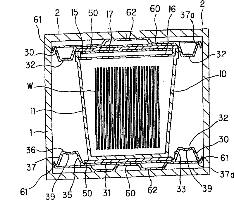
A packaging body that is suitable for transporting contents such as a substrate receiving container, that is not large in size, that has less possibility of contaminating the surroundings, that does not require an increased storage space, and that is less likely to cause problems when reused or recycled. The packaging body has a rectangular tube-like packaging box (1) with the bottom; an upper and lower pair of shock absorbing bodies (30) received in the packaging box (1) while holding the substrate receiving container (10); an elastic body (50) interposed between the substrate receiving container (10) and each shock absorbing body (30); and a reinforcement body (60) for reinforcing each shock absorbing body (30). The shock absorbing body (30) is prepared as a shock absorbing member (31) fitted to the substrate receiving container (10), and a peripheral wall (32) of the shock absorbing member (31) is constructed from an inner wall (35) formed in a bent manner at the peripheral edge ofthe shock absorbing member (31), a projection (36) formed at and projecting from the inner wall (35), and an outer wall (37) formed at the projection (36) and facing the inner wall (35) of the shock absorbing member (31) with a spacing in between. The reinforcement body (60) is formed to have a substantially dish-shaped cross-section, and a bent peripheral edge section (61) of the reinforcement body is fitted and engaged from the outside to an outer wall end section (37a) of the shock absorbing member (31).

Description

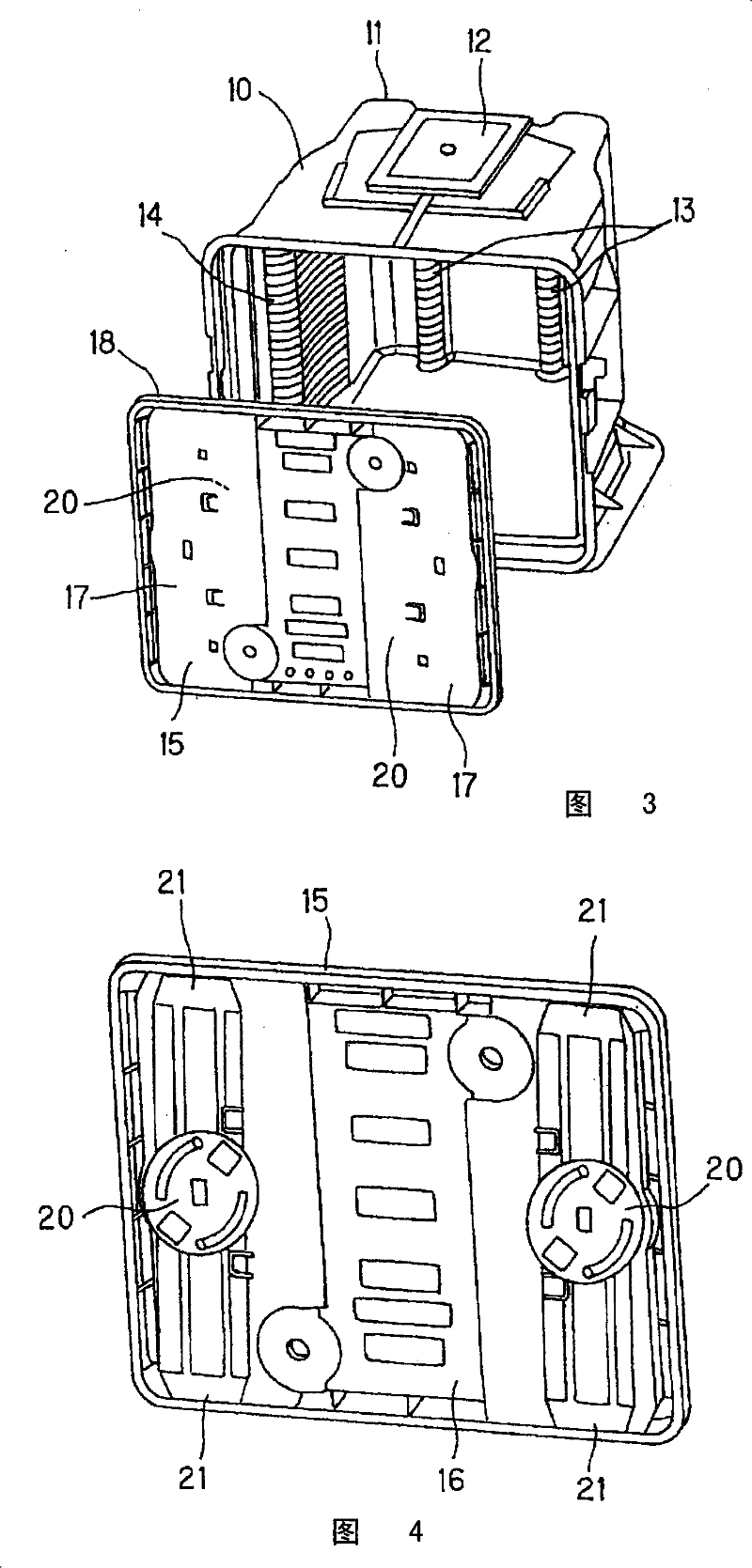
technical field [0001] The present invention relates to a packaging body used when packaging contents composed of a substrate storage container or the like. Background technique [0002] In recent years, semiconductor wafers with a diameter of 300 mm (12 inches) are not the type with a diameter of 200 mm (8 inches), but a type with a diameter of 300 mm (12 inches), and a large-scale dedicated substrate storage container is required to transport wafers of this type. Although not shown in the figure, the substrate storage container actually includes a container body with a front opening box that accommodates a plurality of semiconductor wafers, and a front cover that opens and closes the opening of the container body, and is packaged in a package. transport (refer to Patent Documents 1 and 2). [0003] The lid body is formed, for example, in a horizontally long rectangular shape, and a substantially rectangular front holder that elastically holds the semiconductor wafer accom...

Claims


Application Information

Patent Timeline
Patent Type & Authority Patents(China)
IPC IPC(8): B65D85/86B65D81/107B65D77/26H01L21/673
CPCH01L21/67369B65D77/26B65D81/107B65D85/00H01L21/673
Inventor 恩田武宽中村诚也
Owner SHIN-ETSU POLYMER CO LTD
Learn More