Multi- chip semiconductor device possessing leads and its manufacture method
A semiconductor and multi-chip technology, applied in semiconductor/solid-state device manufacturing, semiconductor devices, semiconductor/solid-state device components, etc., can solve problems such as poor reliability of packages and manufacturing difficulties
- Summary
- Abstract
- Description
- Claims
- Application Information
AI Technical Summary
Problems solved by technology
Method used
Image

Examples
no. 1 example
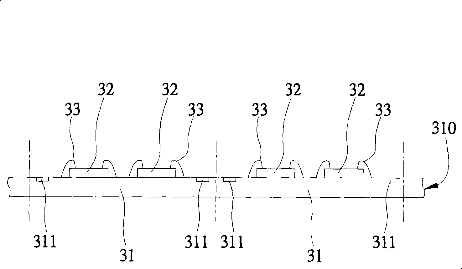
[0046] see Figure 3A to Figure 3E , is a schematic diagram of the manufacturing method of the multi-chip semiconductor device with leads of the present invention, and the following will be described in a batch production method, and of course, it can also be carried out in a single process method.
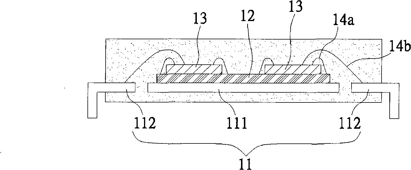
[0047] Such as Figure 3A As shown, a substrate module sheet 310 having a plurality of substrates 31 is provided, and a plurality of connection pads 311 are provided on the surface of each substrate 31 for mounting a plurality of semiconductor chips 32 on the surface of each substrate 31 . The semiconductor chips 32 can be electrically connected to the substrate 31 through bonding wires 33 as shown in the figure, or can be electrically connected to the substrate 31 in a flip-chip manner; the connection pads 311 are disposed on the edge of the substrate 31 .
[0048] Such as Figure 3B and Figure 3C As shown, the encapsulant 34 covering the semiconductor chip 32 and the bonding w...
no. 2 example
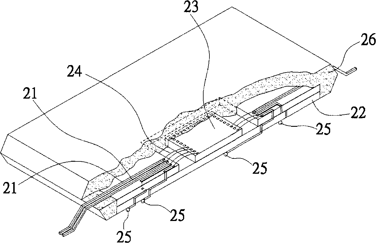
[0055] see Figure 4A and Figure 4B , is a schematic diagram of a second embodiment of the multi-chip semiconductor device with leads and its manufacturing method of the present invention, wherein for the convenience of description and understanding, the same or similar elements corresponding to the previous ones are represented by the same numbers.
[0056] The multi-chip semiconductor device with leads and its manufacturing method in this embodiment are roughly the same as those in the previous embodiments, the main difference is that after the package unit of the chip package is completed and the connection pads exposing the encapsulant are electrically connected to the leads , can also provide a ring reinforcement 41 (such as Figure 4A shown), so that the reinforcing member 41 is connected to the lead 351 through a non-conductive adhesive 42, and the encapsulant 34 of the packaging unit is accommodated in the annular opening 410 of the reinforcing member 41, thereby Th...
no. 3 example
[0058] see Figure 5 , is a schematic diagram of a third embodiment of a multi-chip semiconductor device with leads and a manufacturing method thereof according to the present invention, wherein for the convenience of description and understanding, the same or similar elements corresponding to the previous ones are denoted by the same numbers.
[0059] The multi-chip semiconductor device with leads of this embodiment and its manufacturing method are roughly the same as those of the foregoing embodiments, the main difference being that the packaging unit that completes the chip package and the connection pads that expose the packaging compound and the lead wires of the lead frame are electrically connected. After the permanent connection, a heat sink 51 with a cavity 510 can also be provided, so that the heat sink 51 can be connected to the guide pin 351 through a non-conductive glue 52, and the top surface of the cavity 510 can be separated by a gap. The thermally conductive a...
PUM
 Abstract
Description
Claims
Application Information
 - R&D
- Intellectual Property
- Life Sciences
- Materials
- Tech Scout
- Unparalleled Data Quality
- Higher Quality Content
- 60% Fewer Hallucinations
Browse by: Latest US Patents, China's latest patents, Technical Efficacy Thesaurus, Application Domain, Technology Topic, Popular Technical Reports.
© 2025 PatSnap. All rights reserved.Legal|Privacy policy|Modern Slavery Act Transparency Statement|Sitemap|About US| Contact US: help@patsnap.com