Production method and application of lithium niobate/III family nitride heterojunction ferroelectric semiconductor film

A nitride, heterojunction technology, applied in semiconductor/solid-state device manufacturing, circuits, electrical components, etc., can solve the problems of limited development, difficult integration of ferroelectric oxides, and difficult handling of ferroelectric oxides, and achieves high performance. Battery life, the effect of reducing power consumption

Active Publication Date: 2010-12-08
NANJING UNIV
View PDF1 Cites 0 Cited by
  • Summary
  • Abstract
  • Description
  • Claims
  • Application Information

AI Technical Summary

Problems solved by technology

However, there are still difficulties in the processing of ferroelectric oxides
For example, high processing temperatures and the resulting chemical reactions of the components make ferroelectric oxides difficult to integrate on silicon-based integrated circuits
Difficulties in the integration of ferroelectric materials and silicon-based materials severely limit the development of this field

Method used


Image

  • Production method and application of lithium niobate/III family nitride heterojunction ferroelectric semiconductor film
  • Production method and application of lithium niobate/III family nitride heterojunction ferroelectric semiconductor film
  • Production method and application of lithium niobate/III family nitride heterojunction ferroelectric semiconductor film

Examples


Embodiment Construction

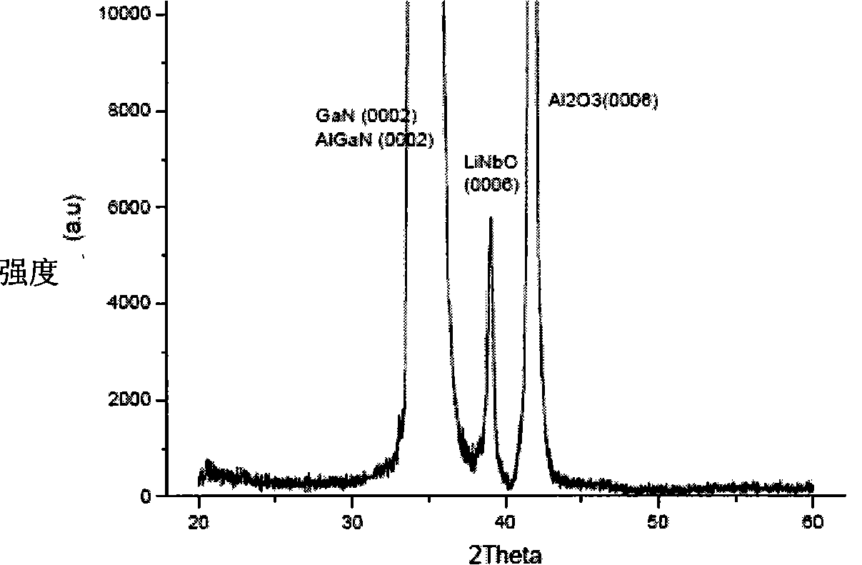
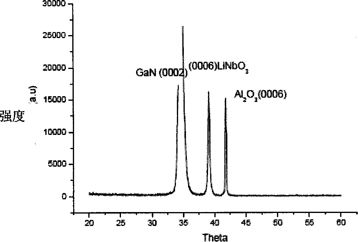
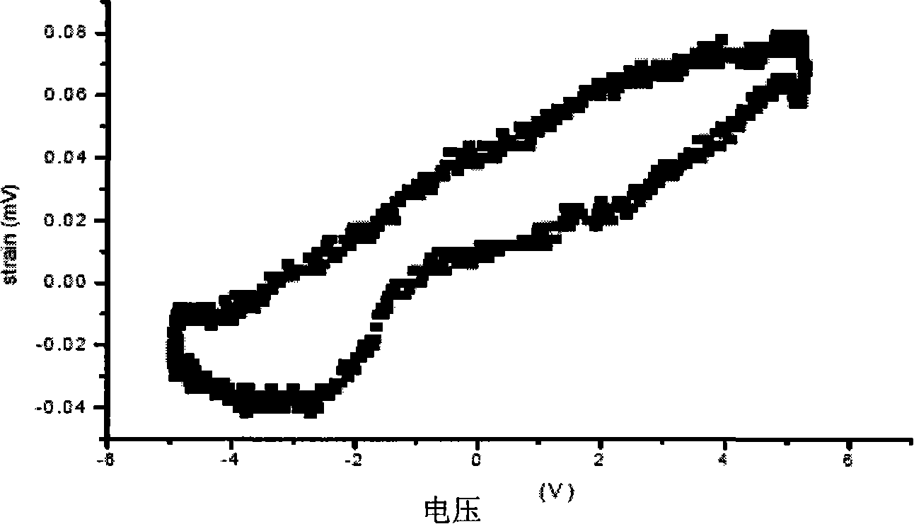
[0029] Using metal organic chemical vapor deposition (MOCVD) to grow group III nitride semiconductor heterostructure materials on (0001) plane sapphire substrates, including AlN / AlGaN, AlN / GaN and AlGaN / GaN heterostructure materials as buffers layers or composite substrates. Through the optimal control of growth conditions such as pulsed laser deposition (PLD) reaction chamber vacuum, growth temperature, and laser energy, the use of high-purity 5N LiNbO 3 Bulk material was used as the target, and high-quality LiNbO was obtained on AlGaN / GaN heterostructure composite substrates by pulsed laser deposition (PLD) 3 film. Then, devices with various functional structures are prepared on the heterostructure thin film through semiconductor device technology.

[0030] 1) AlN / AlGaN, AlN / GaN or AlGaN / GaN heterostructure composite substrates are grown on (0001) plane sapphire substrates by metal organic chemical vapor deposition (MOCVD). Group III nitride semiconductor heterostructure ...


PUM


Abstract

The invention relates to a preparation method of a LiNbO3 / III nitride heterostructure ferroelectric semiconductor thin film, the metal organic chemical vapor deposition method is firstly adopted to grow AlN / AlGaN and other heterostructure materials on a (0001)-plane sapphire substrate as a buffer layer or a compound substrate; then the buffer layer adopts a high-purify 5N ferroelectric material as a target material, the pulsed laser deposition method is used to obtain a high-quality ferroelectric material thin film on the heterostructure buffer layer or the compound substrate; the vacuum of agrowth cavity is controlled to be more than 10<minus 3> Torr; the temperature of the substrate is increased to 300 to 900 DEG C, then high-purity oxygen is introduced into the cavity, the oxygen pressure is controlled at 5 to 90 Pa; the frequency of a laser is adjusted to be 5HZ, the energy is 300mJ, the target material is carried out the laser pre-sputtering in advance for 3 to 5 minutes, and the surface pollution of the substrate is cleaned; finally, the pulsed laser is focused on the target material, and a target source is opened to grow the LiNbO3 / III nitride heterostructure ferroelectricsemiconductor thin film on the heterostructure compound substrate.

Description

technical field [0001] The invention relates to a new method for depositing ferroelectric thin film lithium niobate thin film on group III nitride and heterojunction by using pulsed laser deposition method, especially for preparing ferroelectric semiconductor heterostructure thin film material LiNbO 3 / AlGaN / GaN methods and applications. Background technique [0002] The so-called ferroelectric material means that the crystal structure of the material has a spontaneous polarization phenomenon when no external electric field is applied, and the direction of its spontaneous polarization can be reversed or reoriented by an external electric field. This property of ferroelectric materials is known as "ferroelectricity" or "ferroelectric effect". When a voltage is applied to the crystal, the dipoles align under the action of the electric field. Changing the direction of the voltage reverses the direction of the dipole. This reversibility of the dipoles means that they can repr...

Claims


Application Information

Patent Timeline
Patent Type & Authority Patents(China)
IPC IPC(8): H01L21/8247H01L21/00C23C14/28H01L21/02
Inventor 谢自力张荣严文生修向前韩平陈鹏陆海赵红刘斌李弋宋黎红崔颖超施毅郑有炓
Owner NANJING UNIV
Why Eureka
Try Eureka