Shielding and earthing structure of flexible circuit board

A flexible circuit board and grounding structure technology, applied in the fields of magnetic field/electric field shielding, printed circuit components, electrical components, etc., can solve the problems of long process flow, low manual efficiency, and unsatisfactory shielding effect, and achieve enhanced reliability. performance and electrical performance, and the effect of improving the connection effect

Active Publication Date: 2008-12-10
SHENZHEN XINYU TENGYUE ELECTRONICS
View PDF0 Cites 9 Cited by
  • Summary
  • Abstract
  • Description
  • Claims
  • Application Information

AI Technical Summary

Problems solved by technology

[0005] Technical defects: the process is long, the process control is cumbersome and the difficulty increases and the cost is high, specifically: ①The uniformity of ink debugging directly affects the printing quality; ②The effect of ink thickness control and use; ③The drying temperature directly affects the ink after curing Flexibility and chromatic aberration; ④ The electrical properties cannot be guaranteed stably, the on-resistance is generally above 5 ohms (the best control is within 1 ohm), and the shielding effect is not ideal, etc.
[0007] Technical defects: equivalent to single-layer circuit production, the process is long and unstable, such as: ① increase the number of layers and product thickness, reduce the three-dimensional space; cause friction with the supporting structure, and reduce the service life; ② low manual efficiency , increasing the difficulty of alignment, easy to deviate, higher cost, etc.
[0008] In summary, the above two structural methods have the problems of high cost, high failure rate, and poor protection of shielding effect, which are not compatible with the low cost and high reliability of products required by the market

Method used


Image

  • Shielding and earthing structure of flexible circuit board
  • Shielding and earthing structure of flexible circuit board
  • Shielding and earthing structure of flexible circuit board

Examples


Embodiment Construction

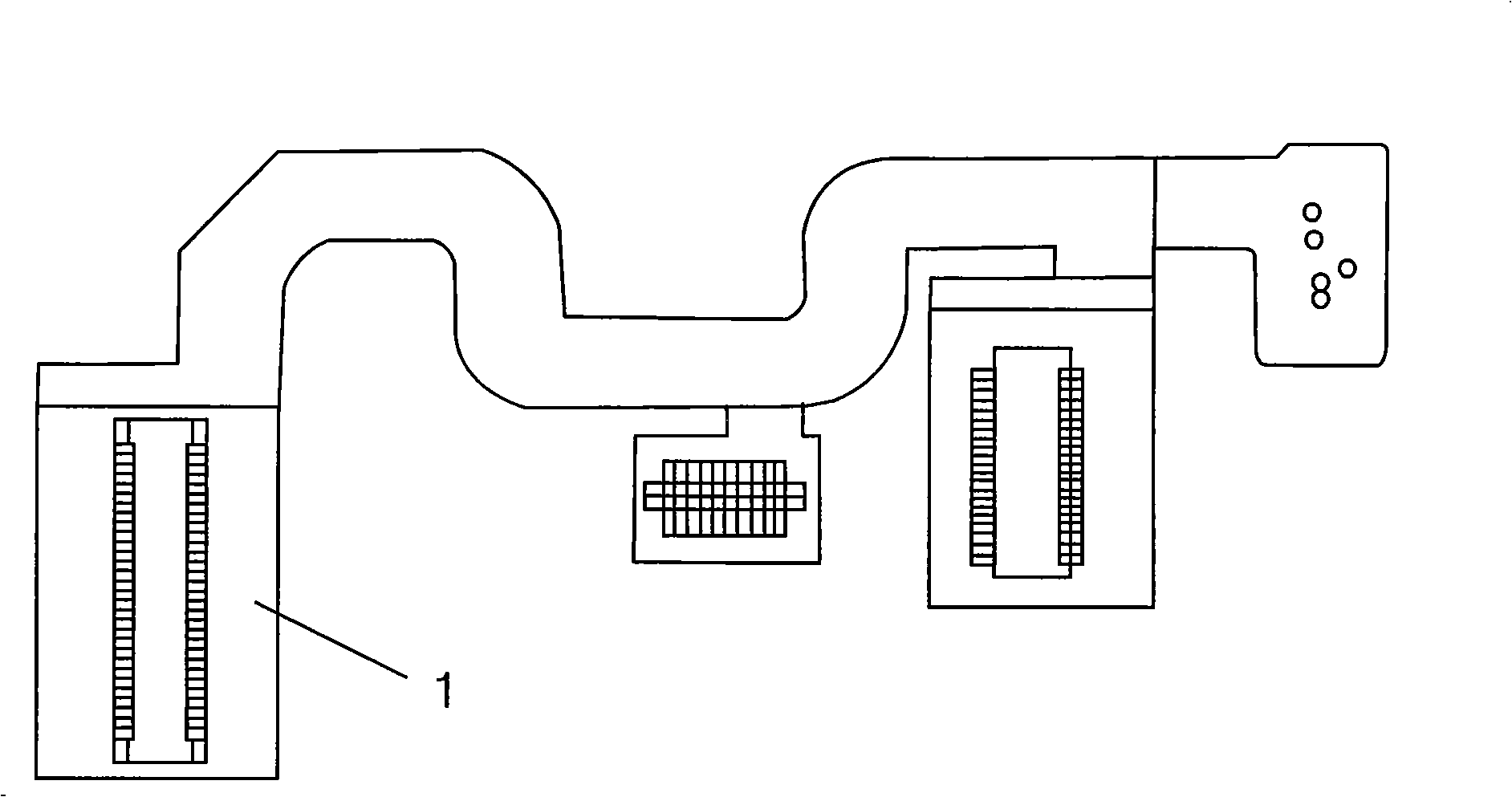
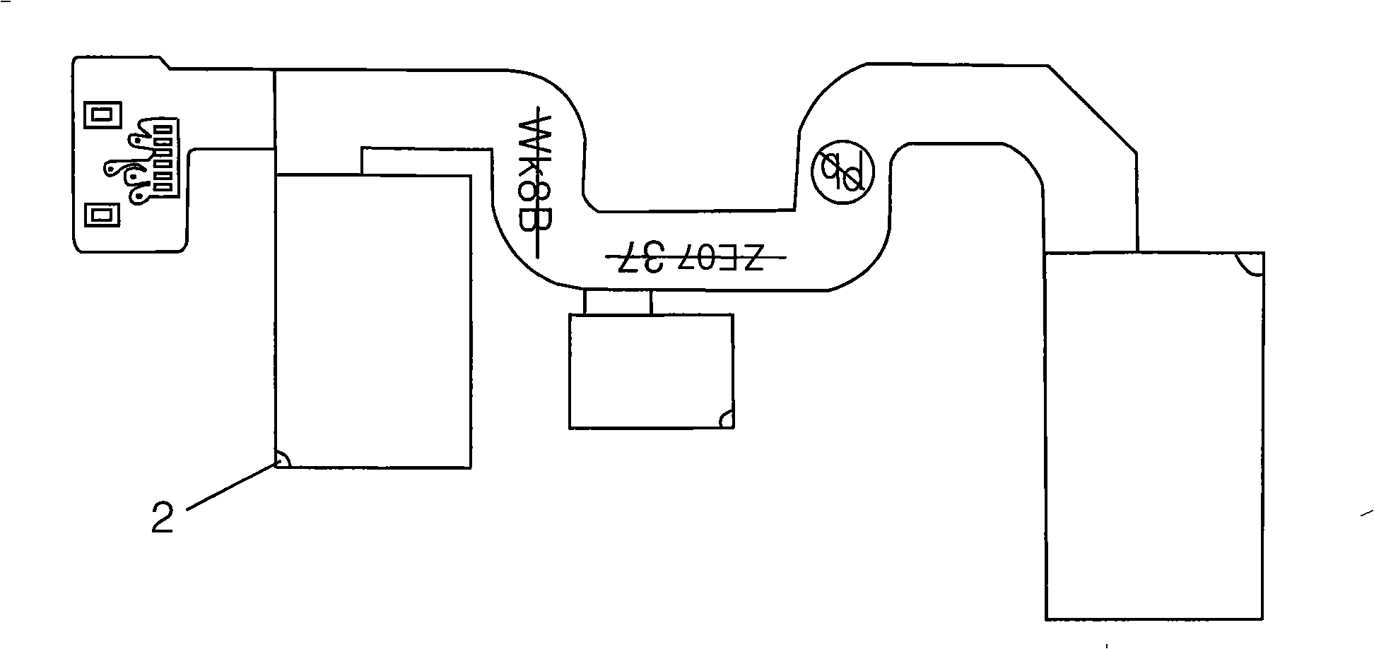
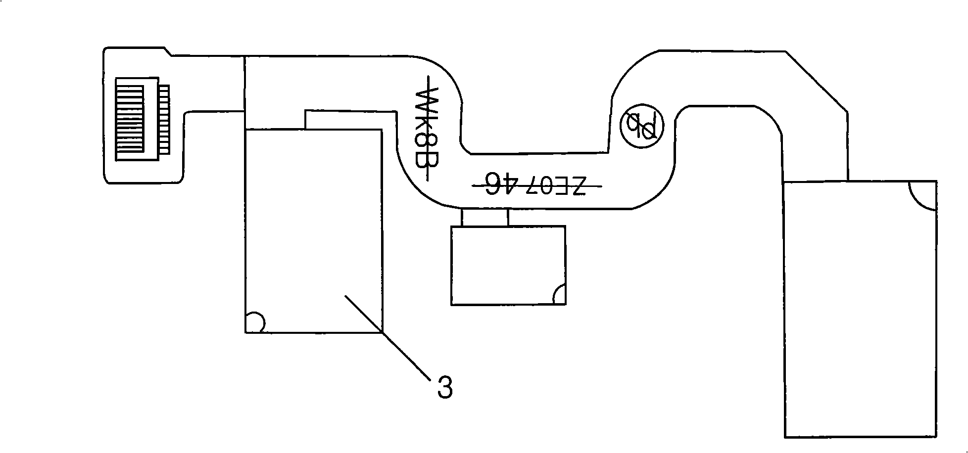
[0024] The present invention will be further described below in conjunction with the accompanying drawings and embodiments. Such as figure 1 and diagram 2-1 , 2-2 As shown, the shielding and grounding structure of the flexible circuit board of the present invention includes the main board 1 of the flexible circuit board, and the grounding copper skin 2 is compounded on the main board 1 through a high-temperature adhesive film, and the grounding copper skin 2 is gold-plated and tinned Finally, a grounding structure is formed, and a conductive shielding film 3 is pressed at a designated position of the main board. Such as Figure 4 As shown, the conductive shielding film of the present invention is composed of an outer release protective film 11, an insulating material 12, a conductor 13, a conductive adhesive 14 and an inner release protective film 15 stacked from top to bottom, and the color can be black or silver. . According to the customer's demand range, add a shield...


PUM


Abstract

The invention discloses a shielding and grounding structure of a flexible circuit board, to realize the aim of high reliability in grounding use, stable electric performance, low cost, good firmness and good appearance effect. In order to solve the technical problem, the invention adopts the following technical proposal: a shielding and grounding structure of a flexible circuit board includes a main board of the flexible circuit board, the main board is compounded with a grounding copper sheet through a high temperature glue film, the grounding copper sheet forms the grounding structure after gold melting and pointing tin, and the appointed position of the main board is pressed with a conductive shielding film. Compared with the prior art, if the conductive resistance is within 1 ohm, the shielding connection effect can be improved effectively, the static electricity can be conducted out in time, thus avoiding burning out other parts to influence the use, and enhancing the reliability and the electric performance of the product greatly.

Description

technical field [0001] The invention relates to a shielding and grounding structure of a flexible circuit board, in particular to a shielding and grounding structure of a flexible circuit board applied to mobile phone communications or products with high-frequency data transmission. Background technique [0002] At present, the shielding materials and processes of Flexible Printed Circuit (FPC) in domestic circuit board factories mostly adopt the structural method of silver paste printing and outer layer lamination of single-sided copper-clad foil. The silver paste used in the first method of printing silver paste is a kind of conductive liquid, which is prepared according to a certain ratio with the curing agent. The slurry contact conducts to ground. At the same time, a layer of yellow insulating ink is printed at a certain position to complete the shielding process and use effect. The second way is to laminate the outer layer with single-sided copper-clad foil. The sing...

Claims


Application Information

Patent Timeline
Patent Type & Authority Applications(China)
IPC IPC(8): H05K1/02H05K9/00
Inventor 张文俊
Owner SHENZHEN XINYU TENGYUE ELECTRONICS
Why Eureka
Try Eureka