Electronic device and method of manufacturing the same

A technology of electronic devices and conductive layers, which is applied in semiconductor/solid-state device manufacturing, electrical solid-state devices, semiconductor/solid-state device components, etc., and can solve problems such as reduced installation reliability

Inactive Publication Date: 2008-12-24
SHINKO ELECTRIC IND CO LTD
View PDF2 Cites 13 Cited by
  • Summary
  • Abstract
  • Description
  • Claims
  • Application Information

AI Technical Summary

Problems solved by technology

Therefore, in the related art semiconductor device, there is a problem that mounting reliability decreases

Method used


Image

  • Electronic device and method of manufacturing the same
  • Electronic device and method of manufacturing the same
  • Electronic device and method of manufacturing the same

Examples


Embodiment Construction

[0052] Hereinafter, exemplary embodiments of the present invention will be described with reference to the accompanying drawings.

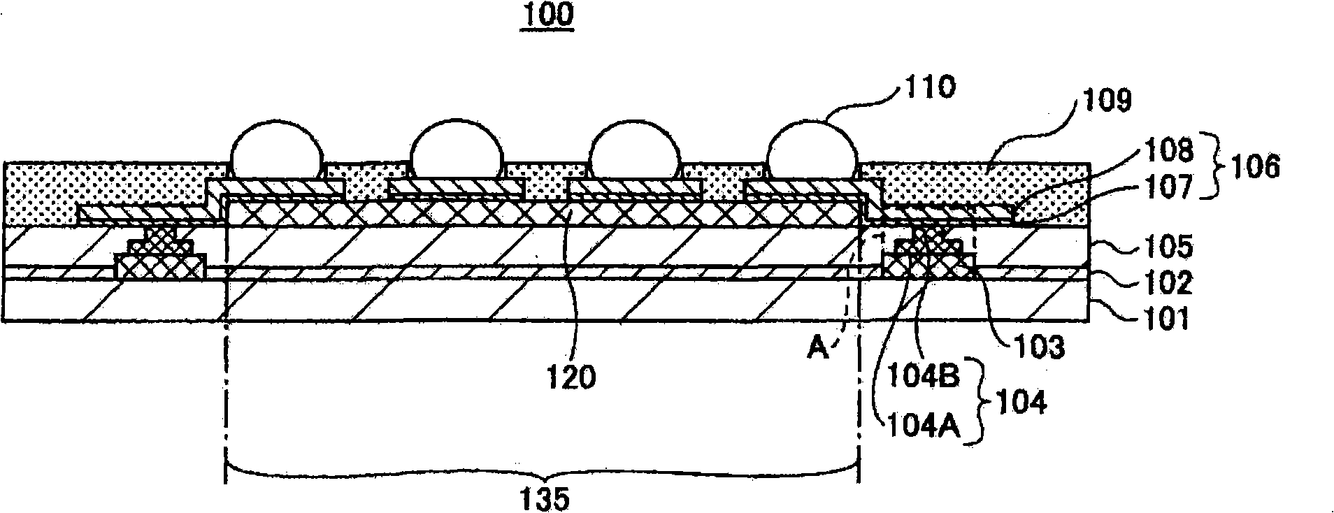
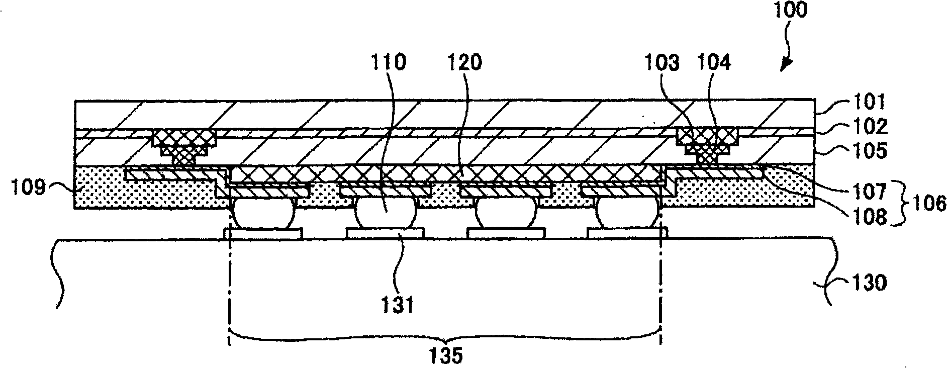
[0053] Figure 1A A semiconductor device according to an embodiment of the present invention is shown. In this embodiment, a chip-level semiconductor device 100 (CSP) is described as an example of an electronic device.

[0054] According to the semiconductor device 100 of the present invention, the electrode pad 103 is formed on the semiconductor chip 101 , and the insulating layer 105 , the stress absorbing layer 120 and the conductive pattern 106 are formed on the passivation layer 102 of the semiconductor chip 101 . In addition, bumps 104 made of gold are also formed on the electrode pads 103 .

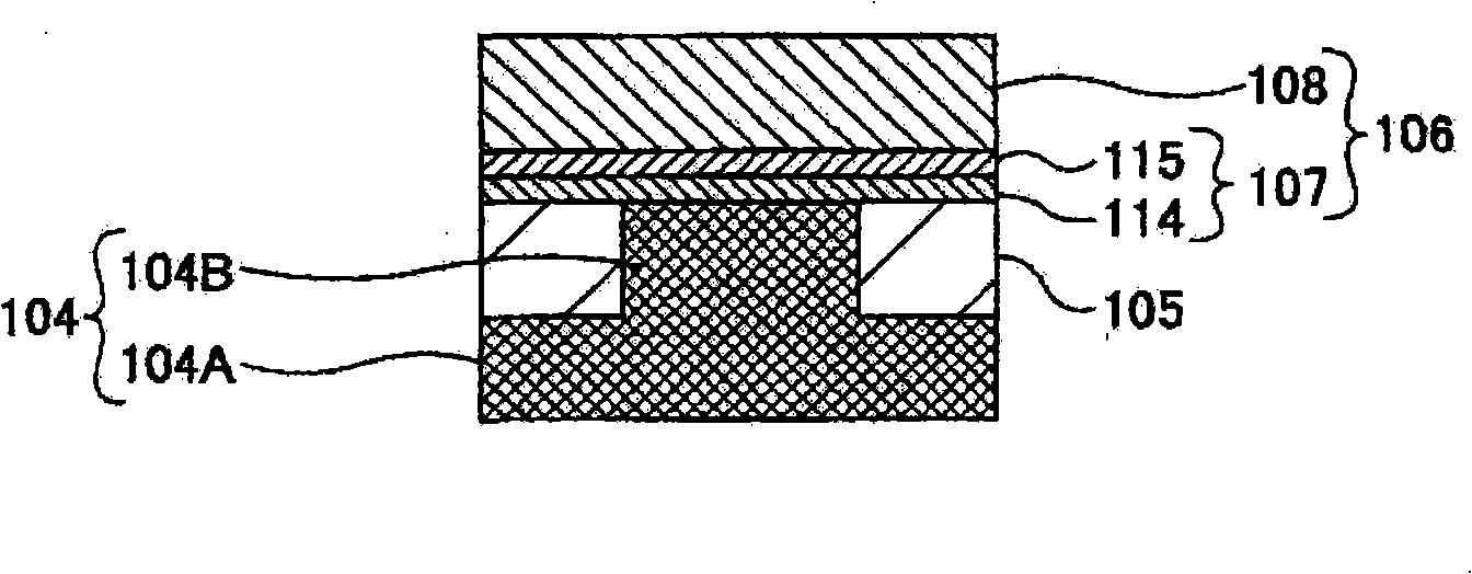
[0055] like Figure 1B As shown, the bump 104 is composed of a bump main body 104A bonded to the electrode pad 103 and a protruding portion 104B protruding from the bump main body 104A. Such bumps 104 are formed with bonding wires made of gold, for ...


PUM


Abstract

The present disclosure relates to a method of manufacturing an electronic device in which a plurality of first bumps serving as external connection terminals are formed on a conductive pattern. The method includes: (a) forming a second bump having a projection portion on an electrode pad formed on a substrate; (b) forming an insulating layer on the substrate; (c) exposing a portion of the projection portion from an upper surface of the insulating layer; (d) forming a flat stress absorbing layer in a bump providing area, in which the first bumps are provided, on the insulating layer; (e) forming a first conductive layer on the insulating layer and the stress absorbing layer and the exposed portion of the projection portion; (f) forming a second conductive layer by an electroplating using the first conductive layer as a power feeding layer; (g) forming the conductive pattern by patterning the second conductive layer; and (h) forming the first bumps on the conductive pattern formed on the stress absorbing layer.

Description

technical field [0001] The present invention relates to an electronic device and a method of manufacturing the electronic device, and more particularly, the present invention relates to an electronic device and a method of manufacturing the electronic device having a conductive pattern formed on an insulating layer having a terminal bumps. Background technique [0002] Various electronic devices have been proposed in which electrodes and conductive patterns are formed on a substrate body such as a semiconductor substrate. As one of the above-mentioned types of electronic equipment, a semiconductor device called a "chip scale package" has been provided. [0003] Chip-scale packaging has a structure in which rewiring (conductive layer) is formed on a device formation surface of a semiconductor chip obtained by dicing a wafer serving as a semiconductor substrate into pieces through an insulating layer (passivation layer) formed in a manner. [0004] For example, when manufac...

Claims


Application Information

Patent Timeline
Patent Type & Authority Applications(China)
IPC IPC(8): H01L21/60H01L23/48
CPCH01L23/3114H01L24/11H01L24/12H01L2224/02313H01L2224/02333H01L2224/02377H01L2224/0401H01L2224/131H01L2924/00013H01L2924/01005H01L2924/01006H01L2924/01015H01L2924/01019H01L2924/01022H01L2924/01024H01L2924/01029H01L2924/01033H01L2924/01037H01L2924/01078H01L2924/01079H01L2924/01088H01L2924/014H01L2924/15788H01L2924/351H01L2224/13099H01L2924/00H01L23/48
Inventor 山野孝治
Owner SHINKO ELECTRIC IND CO LTD
Why Eureka
Try Eureka