Semiconductor device and method for producing the same

A manufacturing method, semiconductor technology, applied in semiconductor/solid-state device manufacturing, semiconductor devices, semiconductor/solid-state device components, etc., can solve the problems of core layer strength reduction, bending, and installation reliability reduction

Inactive Publication Date: 2006-05-31
PANASONIC CORP
View PDF3 Cites 9 Cited by
  • Summary
  • Abstract
  • Description
  • Claims
  • Application Information

AI Technical Summary

Problems solved by technology

However, since the semiconductor element is embedded in the core layer, the thermal stress generated at the bonding portion between the semiconductor element and the base material increases, and as a result, the mounting reliability in the thermal cycle test and the reflow test after moisture absorption is significantly reduced. question
Moreover, if the core layer is formed of a low-elastic material for the purpose of relieving the above-mentioned thermal stress, the strength of the core layer will decrease, and bending and deformation will easily occur.

Method used


Image

  • Semiconductor device and method for producing the same
  • Semiconductor device and method for producing the same
  • Semiconductor device and method for producing the same

Examples


Embodiment approach 1

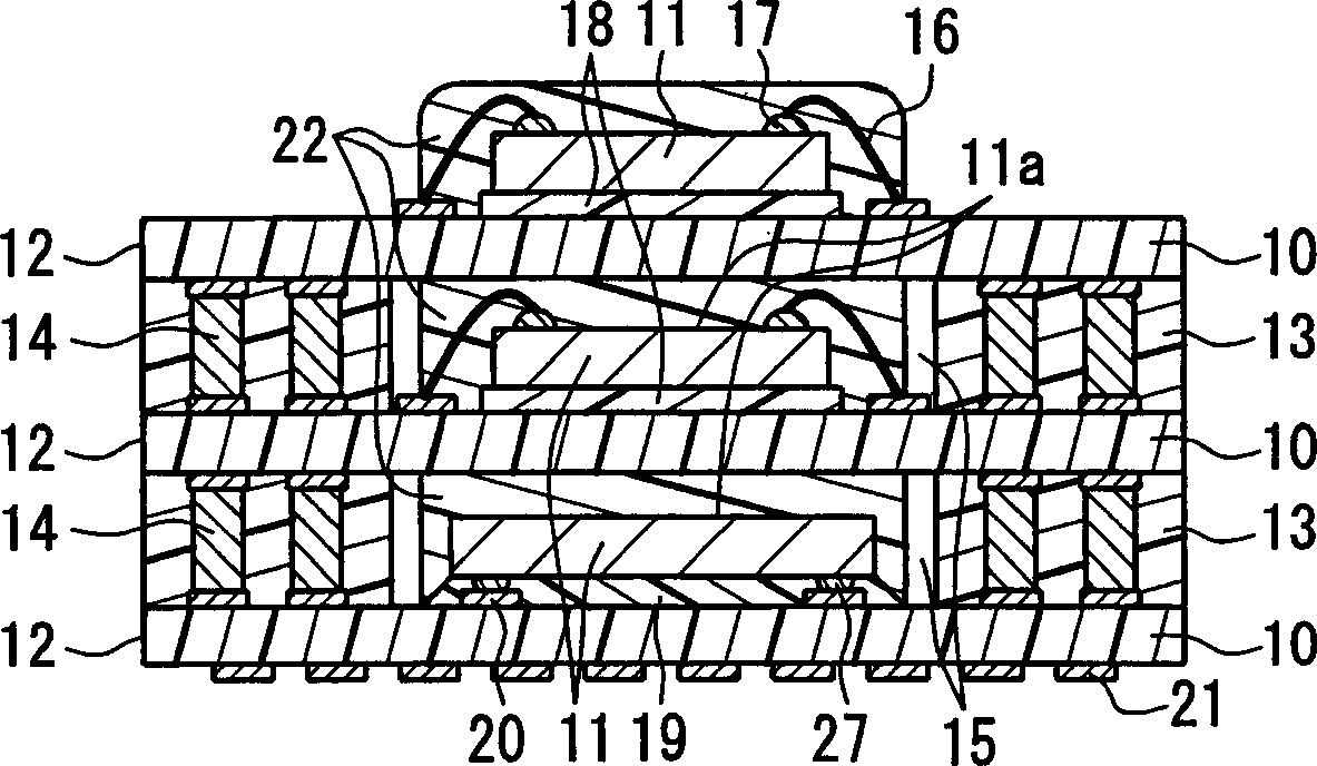
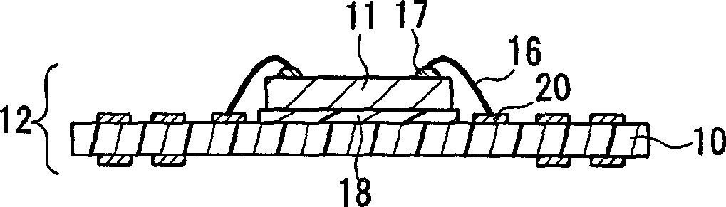
[0061] figure 1 A cross-sectional view of a semiconductor device according to Embodiment 1 of the present invention is shown. Such as figure 1 As shown, the semiconductor device of Embodiment 1 has three circuit boards 12 including a base material 10 and a semiconductor element 11 mounted on the base material 10, and the three circuit boards 12 are connected by a sheet 13 made of a thermosetting resin composition. bonding. These three circuit boards 12 are electrically connected by via conductors 14 penetrating through the sheet 13 , and the semiconductor element 11 arranged between the base materials 10 is housed in the element accommodating portion 15 provided on the sheet 13 . exist figure 1 Among them, 16 is a wire, 17 is an electrode, 18 is a die solder, 19 is an underfill (underfill), 20 is an electrode for component mounting, 21 is an electrode for external connection, and 27 is a gold bump.

[0062] The semiconductor element 11 is not particularly limited, and for ...

Embodiment approach 2

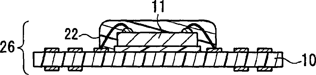
[0089] image 3 A cross-sectional view of a semiconductor device according to Embodiment 2 of the present invention is shown. Such as image 3 As shown, in the semiconductor device of Embodiment 2, all of the semiconductor elements 11 are flip-chip mounted. Moreover, in image 3 On the base material 10 in the middle upper part and the middle part, a through hole 24 communicating with the element receiving part 15 is formed, and on the inner surface of the through hole 24, a connection between wirings to be formed on both main surfaces of the base material 10 is formed. Through conductors 25 for electrical connection between them. Furthermore, a low-elasticity material 22 is filled in the void in the element housing portion 15 . Thus, the semiconductor device of Embodiment 2 has no voids inside it. Others and the above-mentioned semiconductor device of Embodiment 1 (refer to figure 1 )same.

[0090] Since the semiconductor device according to the second embodiment includ...

Embodiment approach 3

[0099] Figure 5 A cross-sectional view of a semiconductor device according to Embodiment 3 of the present invention is shown. Such as Figure 5 As shown, in the semiconductor device according to Embodiment 3, four circuit boards 12 are laminated. Furthermore, through-holes 24 and through-conductors 25 are formed in all base materials 10 . again, in Figure 5 The base material 10 at the bottom and the base material 10 above it are respectively mounted with a semiconductor element 11 accommodated in the element accommodation portion 15, and this group of semiconductor elements 11, 11 is accommodated in the element accommodation portion 15 opposite to each other. . Furthermore, the space in the element housing portion 15 including the portion between the upper surfaces 11a, 11a of the group of semiconductor elements 11, 11 is filled with a low-elasticity material 22 . Other cases and the above-mentioned semiconductor device of Embodiment 2 (refer to image 3 )same. Theref...


PUM


Abstract

A semiconductor device, wherein a plurality of circuit substrates (12) are electrically connected by via conductors (14) penetrating through a sheet (13), and semiconductor elements (11) arranged between substrates (10) are accommodated on the sheet In the component storage part (15) on the material (13), the semiconductor component (11) stored in the component storage part (15) and the surface (11a) opposite to the mounting surface of the semiconductor component (11) are opposite Between the substrates (10), a low-elasticity material (22) having a modulus of elasticity lower than that of the thermosetting resin composition constituting the sheet (13) is filled. Therefore, it is possible to provide a semiconductor device that is less likely to be warped and deformed, and has high mounting reliability.

Description

technical field [0001] The present invention relates to semiconductor devices used in electric and electronic equipment and methods of manufacturing the same. Background technique [0002] As miniaturization of portable electronic devices progresses, miniaturization and high-density assembly of electronic components mounted therein are required. Among various electronic components, a semiconductor device having a multi-stage structure in which circuit boards including semiconductor elements are stacked has been proposed. [0003] As an example of such a semiconductor device with a multi-stage structure, Japanese Unexamined Patent Publication No. 10-135267 proposes a semiconductor device in which circuit boards are electrically connected by ball solder. [0004] However, in the above semiconductor device, since a plurality of packaged circuit boards are stacked, there is a problem that the overall thickness of the semiconductor device becomes thicker. Furthermore, for the p...

Claims


Application Information

Patent Timeline
Patent Type & Authority Applications(China)
IPC IPC(8): H01L25/00H01L21/56H01L21/60H01L23/28H01L23/488
CPCH01L21/563H01L23/3121H01L23/5389H01L25/105H01L2224/16225H01L2224/32225H01L2224/48091H01L2224/48227H01L2224/48465H01L2224/73204H01L2224/73265H01L2224/83192H01L2924/01046H01L2924/01078H01L2924/01079H01L2924/09701H01L24/48H01L2924/01019H01L2924/15311H01L2225/1023H01L2225/107H01L2224/73253H01L2924/3511H01L2224/45144H01L24/45H01L2224/45015H01L2224/45124H01L24/73H01L2924/181H01L2924/1627H01L2924/00014H01L2924/00011H05K3/4697H05K1/186H05K3/4069H01L2924/00H01L2924/00012H01L2924/20752H01L2224/0401
Inventor 平野浩一中谷诚一白石司林祥刚
Owner PANASONIC CORP
Why Eureka
Try Eureka