Polyceramic e-chuck

a polyceramic, e-chuck technology, applied in the direction of electrostatic holding devices, manufacturing tools, mechanical apparatuses, etc., can solve the problems of inpracticality of charging and discharging periods, inability to charge and discharge, and inability to use precision, so as to improve the control of the capacitance budget, reduce thermal stresses, and reduce capacitance

Active Publication Date: 2009-01-01
FM INDS
View PDF17 Cites 61 Cited by
  • Summary
  • Abstract
  • Description
  • Claims
  • Application Information

AI Technical Summary

Benefits of technology

[0018]Another important advantage of the invention is that the use of a polymer as a bottom layer dielectric, when adhered to a metal base, does not require thermal matching between a ceramic and a metal when bottom dielectric is a ceramic, as is the case with most conventional chucks. According to the present invention, the polymer adhesive layer can expand or contract independent of the ceramic thereby reducing thermal stresses.
[0019]Some known electrostatic chucks may use ceramics as their top and bottom layer dielectric. According to embodiments of the present invention, the top layer comprises a ceramic, however the bottom dielectric layer is a polymer. Preferably, the polymer is filled with a ceramic. This polyceramic layer allows for better control of capacitive budget in a given application. The polymeric layer also provides relief of stresses from a potential differential thermal expansion of the top ceramic layer and the bottom metal heat sink. The polyceramic structure can be bonded to a metal, and the metal can be protected by a thermal sprayed coating of a dielectric material such as, for example, alumina, yttria, magnesia, titania and other alloyed dielectric ceramics, etc.
[0020]The electrostatic chucks of the present invention control capacitive load presented by a chuck in a semiconductor chamber. By reducing capacitance, the reactive capacitance component is decreased, thus easing the typical difficulty in matching the RF load of various components. The chucks of the present invention may be manufactured at a lower fusion temperature compared to conventional chucks, leading to a significantly lower manufacturing times and commensurate manufacturing cost. The use of polymer or ceramic filled polymer adhesive allows the layers in the chuck to be bonded to a heat sink without the need for matching the thermal expansion of the component layers. Most materials that have low thermal expansion also have lower thermal conductivity, as such thermal matching to ceramics also reduces thermal conductivity of the heat sink. If thermal matching is not required in a manufacturing process for chucks, then materials with high thermal conductivity can be selected for heat sink, as proposed in embodiments of this invention.
[0021]The polyceramic chucks of the present invention can provide a low cost solution to chuck manufacturing, as such chucks require lower compensation for capacitive reactance, thereby reducing cost of the RF matching network. The chucks of the present invention have anti-arc features that provide long life and low 
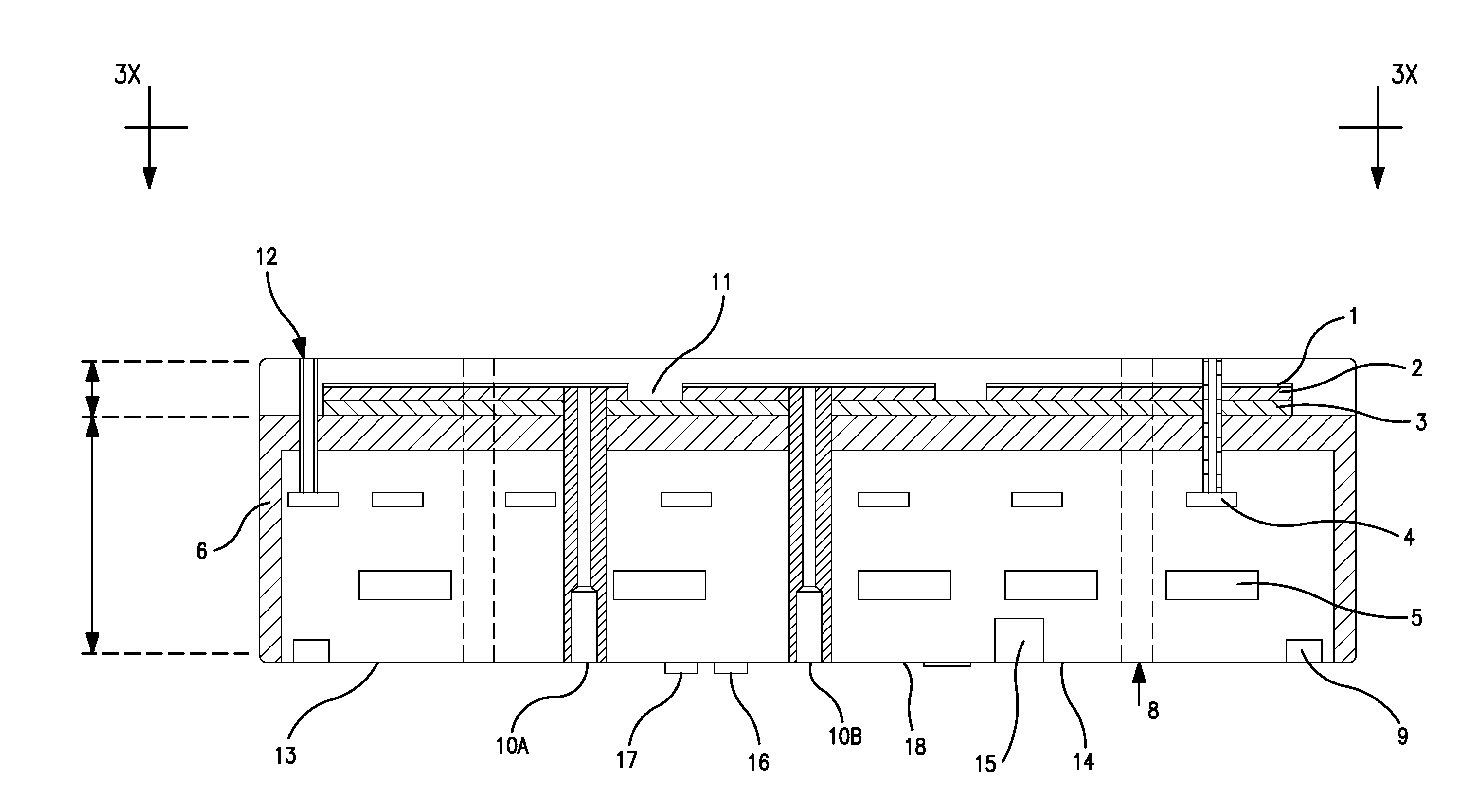
cost of ownership. FIG. 1 shows, in cross-section, a preferred polyceramic e-chuck made according to preferred embodiments of the present invention. Such a structure can be manufactured by using a sintered ceramic top dielectric layer (1) made of aluminum oxide of at least about 99.5% purity with an isolation rib structure (11) machined to provide for electrical isolation to segmented electrodes (2). The electrodes (2) are deposited by sputtering tungsten within the isolation rib structure (11). Electrodes may also be formed by metallization of the ceramics. The electrode (2) is then encapsulated with a polyceramic adhesive (3) and this ceramic, metal and polyceramic layered structure is then bonded to the metal heat sink (14). The heat sink (14) is made of 6061Al or other suitable thermally conductive alloy. The heat sink comprises cooling gas channels (4) that are fed with a cooling gas from an inlet (18) at the base of the heat sink. The heat sink is brazed to form a cooling fluid channel (5) that has inlet (16) and outlet (17) for connections to a thermal controller, such as, for example, a chiller. The heat sink is coated with a layer of a dielectric material like aluminum oxide using a thermal spray device referred to as anti-arc coating (6). Dielectric material, such as, for example, a sintered ceramic, or thermal spray coating may be used on the top surface (19) of the heat sink (14). The backside or the areas of the aluminum heat sink exposed to low voltages are anodized (13). The bonded ESC is connected to DC power pins (10A) and (10B) through the heat sink (14). The power pins (10A, 10B) are used to energize the segmented electrode (2). One or more power pins may be used for the corresponding segmented electrodes as required for a monopolar or multipolar e-chuck. The heat sink (14) has thru holes (8) for lift pins. These thru holes are preferably lined with a dielectric material like aluminum oxide. The electrostatic chucks are used in vacuum chambers as such they require O-rings (9) to seal the chamber against atmosphere. The heat sink (14) has a provision for application for RF connection (15).
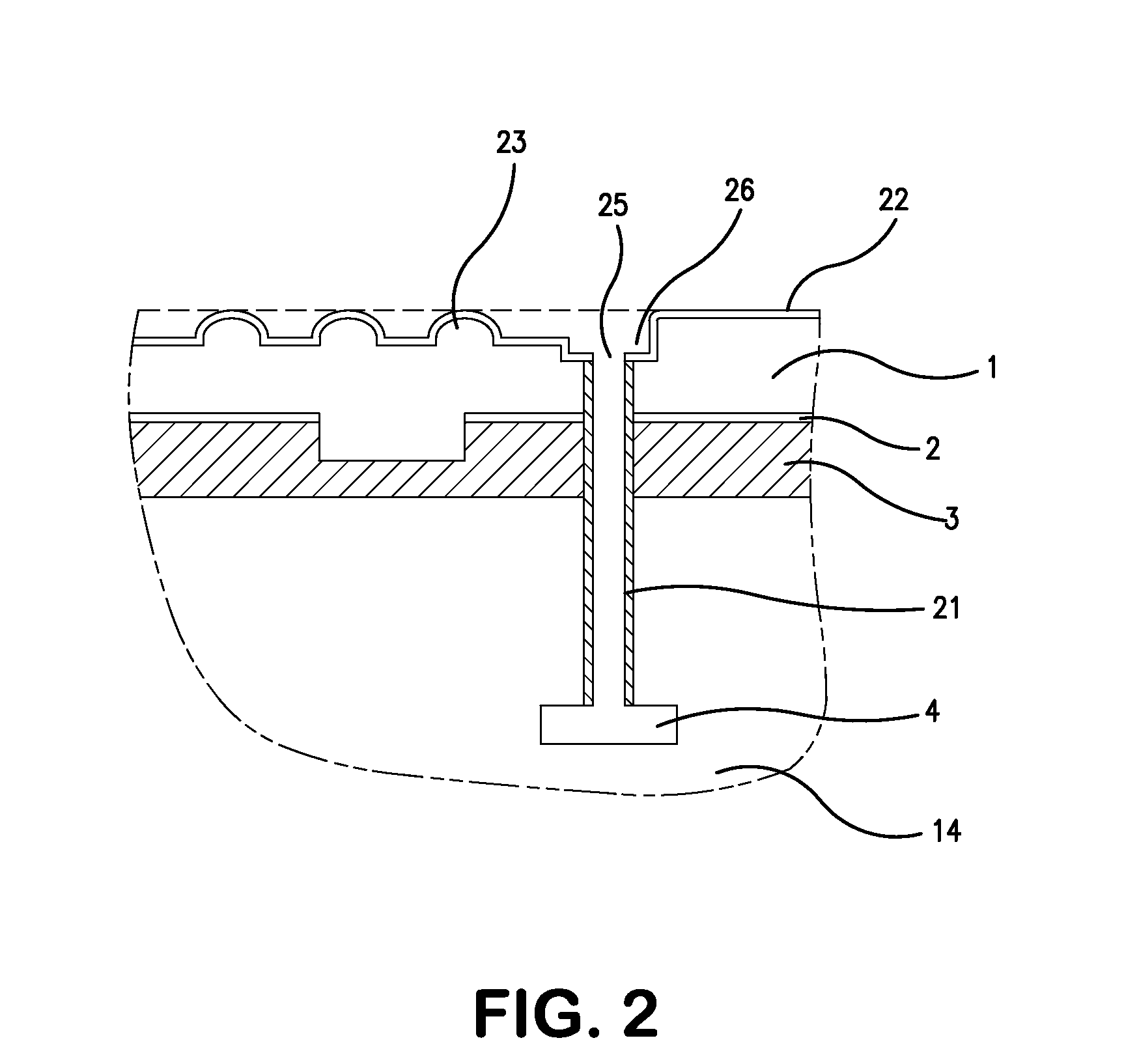
[0022]FIG. 2 shows details of the wafer clamping surface in cross-section. In addition a key feature of this invention is shown where the cooling gas passage is lined with a dielectric material (21), for example, a ceramic or a polymer. The presence of a dielectric insert inside the gas holes (25) prevents arcing to the base metal or heat sink (14) from any plasma arcing that may develop underneath a wafer due to the bias voltage imposed on the wafer. Another key feature of the invention shown is the mesa structure (23) along with gas grooves (26) on the wafer clamping surface (22). The mesa structures (23) are integral parts of the top dielectric surface. However, mesa structures (23) also may be deposited on the dielectric surface by various thin film deposition techniques like PVD or CVD, as would readily be understood by those skilled in the field of thin film material deposition. Integral mesa structures (23) may be encapsulated in conformal films, with such films made from materials including, for example, carbon, silicon dioxide, silicon nitride, aluminum nitride, polyimid, flouorocarbons of siloxanes, combinations thereof, etc.
[0023]Mesa structures are provided to reduce the area of contact in a range of from about 1% to about 25%. The reduction in contact area results in a decrease in clamping force, but provides an advantage to gain quick release time. The mesa structure also reduces the number of particles transferred to the backside of a wafer, due to decrease in area of contact. In addition, mesa structure allows for, among other things, distribution of cooling gas behind the wafer surface during wafer clamping, thus enhancing heat transfer from the wafer to the top dielectric surface.

Problems solved by technology

Such chucks eliminate the need for the prior used mechanical clamping devices that were often difficult to use with precision, and often introduced contaminants to the semiconductor manufacturing chambers.
However such known designs have prolonged charging and discharging periods of up to 10 seconds or longer.
Such charging and discharging periods are viewed as impractical in most modern semiconductor manufacturing processes that require faster throughput.
Indeed, metal bases in the chuck construction are prone to electrical bridging or arcing that can result in leakage between electrodes and the base.
Such arcing can drain off the stored charge that holds the work piece in place, and exposed metal base results in arcing damage in plasma chambers.
Known chucks have not provided such a desired reduction.
Further, the problem of arcing with known electrostatic chucks has not been completely addressed as metal base heat sink arcing typically occurs to some extent.

Method used


Image

  • Polyceramic e-chuck
  • Polyceramic e-chuck
  • Polyceramic e-chuck

Examples


example 1

[0026]In one preferred method of the present invention, the top layer is made from a ceramic aluminum oxide that is at least about 99.5% in purity, with a dielectric constant of from about 8.5 to about 9.5, a resistivity of 1E12 ohm.m. and a breakdown voltage of 22 KV / mm. An electrode comprises tungsten (W) with a resistivity of about 0.06 micro-ohm-m. The preferred electrode can be a single pole, or the electrode is segmented to create poles that are preferably even in number and have equal area and hence equal capacitance. A bottom dielectric is made of a polyceramic layer with a dielectric constant of 3.5, a resistivity of about 1E15 ohm.m and a breakdown voltage of 300 KV / mm. The polyceramic was made of a siloxane compound filled with aluminum oxide. Such an assembly was manufactured and tested on a heat sink made of 6061 T6 aluminum. A 300 mm Si wafer was clamped in a vacuum chamber. Aluminum oxide thermal sprayed layer was used on the exposed surfaces of the heat sink to preve...

example 2

[0027]In another preferred assembly method a ceramic aluminum oxide about (99.5%) was used as the top dielectric with a dielectric constant of greater than about 8, a resistivity of 1E15 ohm.m and a breakdown voltage of about 22 KV / mm. An electrode was made from tungsten (W) with a resistivity of 0.06 micro-ohm-m. The bottom dielectric was made of polyimid having a dielectric constant of 3.5, a resistivity of 1E16 ohm.m and a breakdown voltage of 300 KV / mm. Such an assembly was manufactured and tested on a heat sink made of 6061 T6 aluminum. A 300 mm Si wafer was clamped in a vacuum chamber.

[0028]In further examples, a chuck was made with the same structure as defined above, where the polymeric filler was boron nitride. In yet further examples, a chuck was made with the same structure as defined above, where the polymeric filler was aluminum nitride.

[0029]In still further examples, a chuck was made with a top dielectric made of silicate glass with a dielectric constant of 6.5, with ...


PUM


Abstract

The present invention discloses an electrostatic chuck for clamping work substrates, said chuck comprising three layers, where the dielectric constant of included non-conductive layers is selected to provide overall lower capacitance to the chuck. In the chuck assembly of the present invention, the top dielectric layer that is in contact with a substrate, such as, for example, a wafer, has a dielectric constant that is preferably greater than about 5, with a resistivity that is preferably greater than about 1E6 ohm.m, whereas the bottom dielectric layer has a dielectric constant that is preferably less than about 5 and a resistivity that is preferably greater than about 1E10 ohm.m. The intermediate layer preferably has a conductive layer where the resistivity is less than about 1 ohm.m. The electrostatic chuck may be bonded to heat sinks coated with anti-arc dielectrics. The heat sink can also be used as an RF electrode. The heat sink may have provisions for coolants and gas channels to feed a cooling gas to the backside of a wafer. The heat sink may have feed thrus to power the segmented electrodes in the electrostatic chuck. The passages for the feed thrus, gas feed holes and lift pins may be lined with ceramics or polymers to prevent any discharge to the heat sink. The electrostatic chuck is for clamping work substrates like Si, GaAs, SiO2, etc. used in semiconductor tools.

Description

FIELD OF THE INVENTION[0001]The present invention, in general, is directed to electrostatic chucks (e-chucks) for use in semi-conductor manufacturing. More specifically, the present invention is directed to the use and manufacture of improved multilayer electrostatic and ceramic chucks, each layer preferably having varying dielectric constants and resistivities.BACKGROUND OF THE INVENTION[0002]Electrostatic chucks are known devices used in semiconductor manufacturing processes. Such chucks eliminate the need for the prior used mechanical clamping devices that were often difficult to use with precision, and often introduced contaminants to the semiconductor manufacturing chambers. Chucks support the substrates within the semiconductor wafer manufacturing or processing chamber. Designers have developed electrostatic chucks that comprise ceramics in combination with an embedded metallic conductor. These chucks are often referred to as “ceramic chucks”. Ceramic chucks hold an electrosta...

Claims


Application Information

Patent Timeline
Patent Type & Authority Applications(United States)
IPC IPC(8): H02N13/00B23B5/22H01T23/00
CPCH01J2237/2007H01L21/67109H01L21/6831Y10T279/23H01L21/68757H02N13/00H01L21/6875
Inventor NAIM, MAHMOOD
Owner FM INDS
Why Eureka
Try Eureka