Method and structure to prevent distortion and expansion of organic spacer layer for thin film transfer-join technology

a technology of organic spacer layer and transfer-joining, which is applied in the direction of fixed connections, sustainable manufacturing/processing, final product manufacturing, etc., can solve the problems of shrinkage, even distortion, and shrinkage of the active thin film structure area, and achieve high wiring density, reduce thermal stress, and reduce distortion of the thin film.

Inactive Publication Date: 2001-12-11
IBM CORP
View PDF17 Cites 60 Cited by
  • Summary
  • Abstract
  • Description
  • Claims
  • Application Information

AI Technical Summary

Benefits of technology

The above and other objects and advantages, which will be apparent to one of skill in the art, are achieved in the present invention which is directed to, in a first aspect, a joined electronic component assembly structure having reflowed solder bump attach between the two electronic components which is cost effective and reliable. The structure comprises a carrier component such as a multilayer ceramic substrate (MLC) with a top surface and an array of electrical contact pads patterned on the carrier surface and a multilayer thin film electronic component wherein contact pads on its bottom surface correspond to and are connected to the contact pads on the top surface of the carrier by reflowed solder bumps. A spacer of non-conductive, compliant material is interposed between the bottom surface of the thin film and the top surface of the carrier. The spacer has through-vias (or through-holes) arranged in a pattern corresponding to the array of pad contacts on each component so that one array of pad contacts is on one side of the through-holes and the other array of pad contacts is on the other side of the through-holes. At least one of the electronic components has opposed contact pads, and preferably both components have opposed contact pads, comprising a thick film of metal thereon (typically in the form of a post or other protrusion) which extends above the contact pad surface and extends partly into the through-hole opening of the spacer when the electronic components are joined. After solder-join, the reflowed solder connection extends through the spacer through-holes and connects opposing pairs of pad contacts on the thin film and MLC carrier, with the posts being embedded in the reflowed solder joint. Not all the opposed contact pads of each component need the thick film of metal or post but preferably at least 10% of the pads and most preferably greater than 50% will have the metal or post thereon. It is also preferred that the corresponding pads of each component have the post thereon.
In accordance with another aspect of the present invention, the carrier, to which the thin film is bonded, is either a multilayer ceramic substrate or a laminate structure such as a printed circuit card. The solder connections are formed by reflowing opposing pairs of solder balls and posts on the carrier and the thin film using any solder reflow process such as a closed solder joining process. The thin film is typically built on a first sacrificial carrier, and then further processed by securing it to a second sacrificial carrier. The second sacrificial carrier reduces distortion of, damage to, and surface topography on the thin film during its bonding to the destination carrier and other related processing.
The spacer is then placed on either the exposed metal post containing surface of the thin film or on the solder-bump surface of the ceramic substrate or printed circuit card with the through-holes aligned with the metal posts and solder bumps. The solder bumps of the substrate or card are positioned to oppose and align with corresponding metal posts of the thin film, thereby forming opposing pairs of the corresponding metal posts and solder bumps. In one process of solder reflow joining, heat of less than 400.degree. C. and inward pressure of less than 200 psi are applied to the assembly in a closed solder joining process, thereby causing the solder bumps to reflow and form new solder connections between the now joined components. Nonsolder areas are also typically bonded to provide physical support for the thin film. This is typically accomplished using an adhesive layer on the spacer. After the solder connections are formed, the second sacrificial carrier of the thin film is generally removed for attach of a chip or other electronic component to this surface of the thin film structure. The resulting structure comprises a thin film electronic component structure which is mechanically bonded and electrically connected to a MLC substrate or card, and which has been processed using a method which reduces distortion of, damage to, and topography variations on the thin film.
In accordance with another aspect of the present invention, the thin film is adhered to a portion of a printed circuit card to form a region of high wiring density. A chip is then secured to the top surface of the thin film. A spacer is interposed between the card and the thin film which reduces thermal stresses on the chip secured to the thin film and with the contact pad posts of the invention provides a reliable solder reflow bond. Adhesive on the spacer and reflowed solder column patterns can be varied between the spacer, thin film, and laminate card to vary the nature of the solder joints and thermal stress reduction.

Problems solved by technology

The prior art processes of achieving active pad connections with thin film components have drawbacks and disadvantages however.
Many of the drawbacks and disadvantages of this approach relate to the fact that the thin film is released from its sacrificial carrier in a free-standing form before lamination joining with the MLC.
The shrinkage of the thin film makes it difficult to align the pads and other electrical connections of the thin film to the corresponding MLC carrier.
Such shrinkage, and even distortion, are exacerbated if the thin film structure is released from its sacrificial carrier too soon in the manufacturing process.
The solution of holding the thin film around its edges with a ring or frame after release has the additional disadvantage of reducing the active thin film structure area.
A consistent obstacle in attaching chips to laminate substrates is the mismatch of the thermal coefficient of expansion, or TCE, between the chips and the laminated boards or substrates.
This problem is especially acute in the case of direct chip attach.
Regardless of the electronic components being joined, the mismatch of TCE between the two components generates shear stress on the electrical connections between the components and such shear stresses result in fatigue of the connections over the life of the product, making those connections prone to failure.
In addition, the difference in the TCE applies bending forces to the components at their outer edges and, therefore, may cause the components to crack.
Unfortunately, the foregoing use of underfill is unworkable for joining two components which are large (typically greater than 25 mm) due to inability of the underfill to flow under such large areas.

Method used


Image

  • Method and structure to prevent distortion and expansion of organic spacer layer for thin film transfer-join technology
  • Method and structure to prevent distortion and expansion of organic spacer layer for thin film transfer-join technology
  • Method and structure to prevent distortion and expansion of organic spacer layer for thin film transfer-join technology

Examples


Embodiment Construction

)

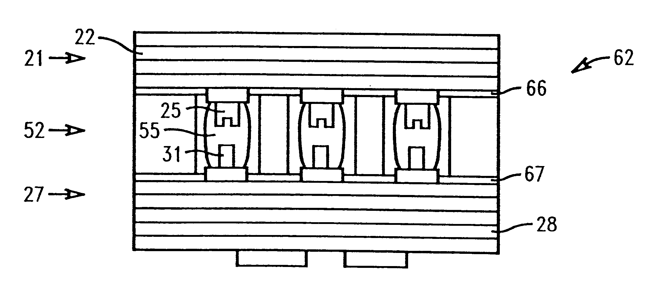
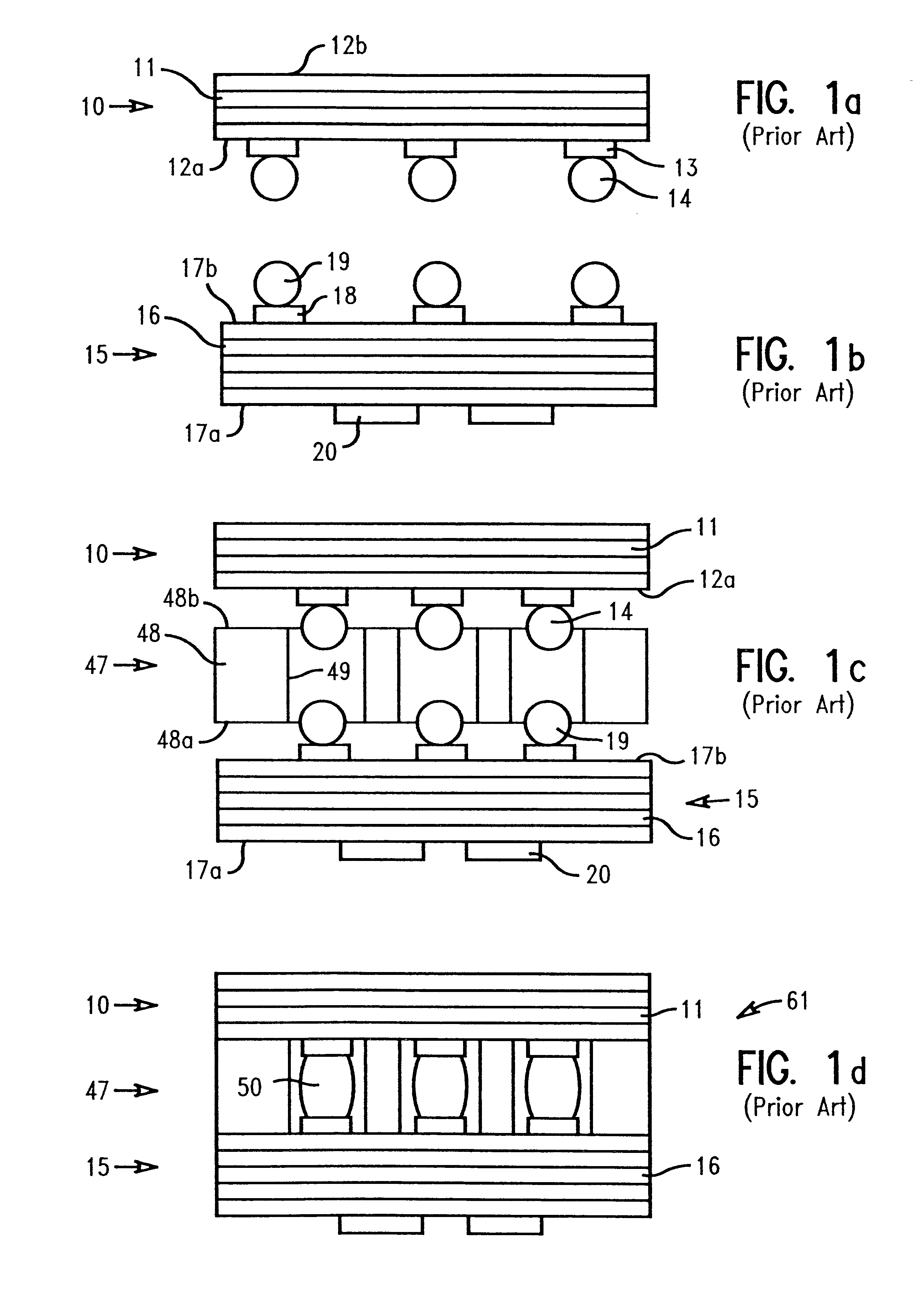
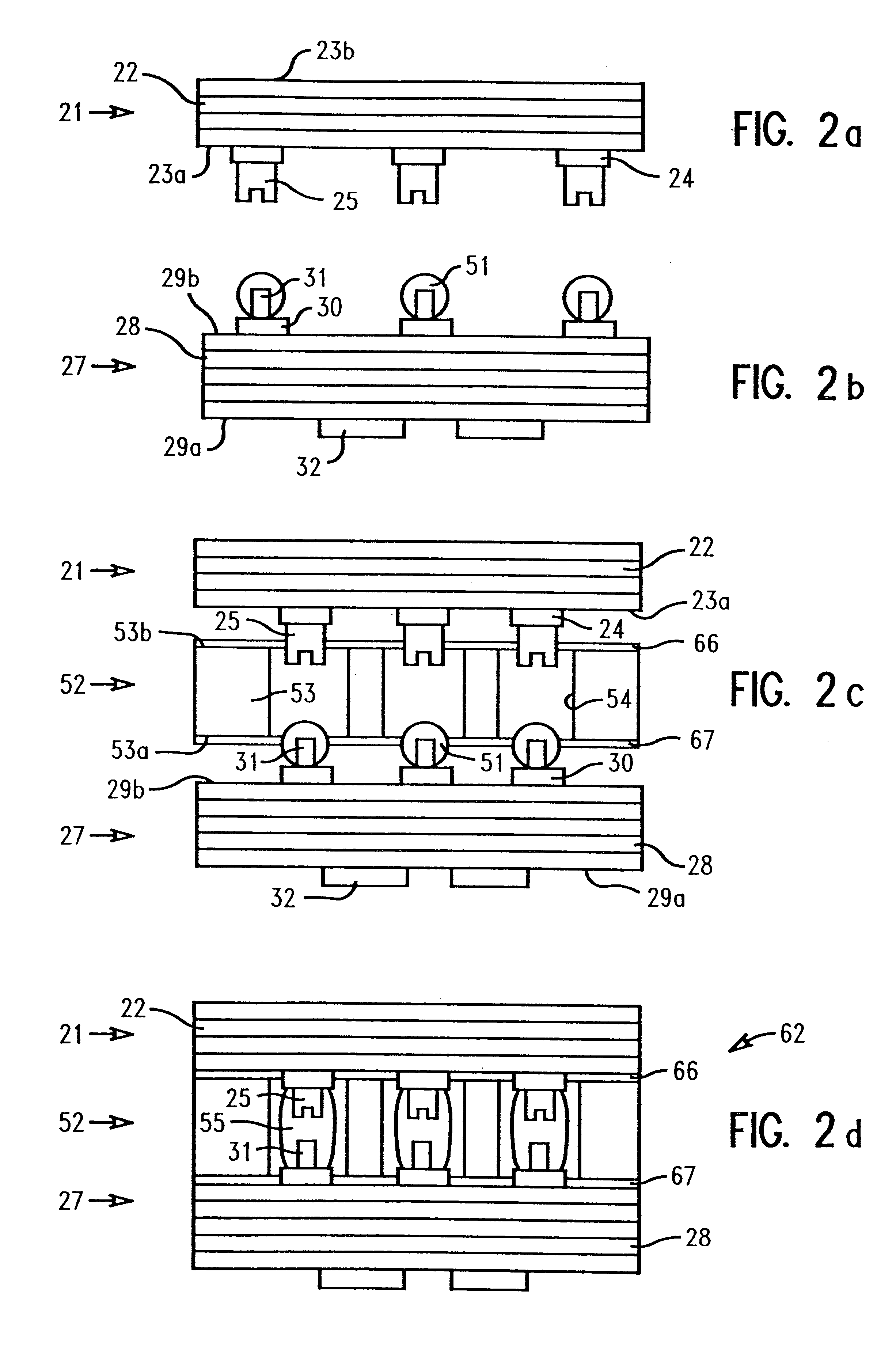
In describing the preferred embodiment of the present invention, reference will be made herein to FIGS. 1a-3d of the drawings in which like numerals refer to like features of the invention. Features of the invention are not necessarily shown to scale in the drawings.

While the following description will be specifically directed to joining a thin film structure to a multilayer ceramic structure it will be appreciated by those skilled in the art that any two electronic components having corresponding contact pads and solder bumps thereon for joining may be formed using the method of the invention.

Referring now to FIG. 1a, a thin film structure is shown generally as numeral 10. The thin film structure comprises a series of thin film layers shown in composite as 11, and as well known in the art, the layers are interconnected with vias and wiring. The thin film structure is shown so that pads 13 having solder bumps 14 thereon are shown on the lower surface indicated as 12a. The opposed s...


PUM

PropertyMeasurementUnit
thicknessaaaaaaaaaa
pressureaaaaaaaaaa
thicknessaaaaaaaaaa

Abstract

An electronic component structure assembly comprising a thin film structure bonded to a multilayer ceramic substrate (MLC) using solder connections and wherein a non-conductive, compliant spacer preferably with a layer of thermoplastic adhesive on each surface thereof is interposed between the underlying MLC carrier and overlying thin film structure. The spacer includes a pattern of through-holes which corresponds to opposing contact pads of the thin film structure and MLC. The contact pads of at least one of the thin film structure or MLC have posts (e.g., metallic) thereon and the posts extend partly into the spacer through-holes whereby the height of the posts are greater than the thickness of the adhesive. The posts of the MLC have solder bumps thereon. After reflow under pressure the thin film structure is electrically and mechanically connected to the MLC and the join method has been found to provide a reliable and cost-effective process. The joined components also have enhanced operating life.

Description

1. Field of the InventionThe present invention relates generally to electronic device assemblies wherein one electronic component is mechanically and electrically bonded to another electronic component and, more particularly, to assemblies comprising a copper-polyimide "thin film" electronic component structure and a multilayer ceramic substrate electronic component structure with an organic spacer between the components to align the contact pads of each component, which structures are mechanically and electrically bonded together by solder reflow and to a method for making the assembly without defective solder connections and increased reliability and cost-effectiveness of the manufacturing process.2. Description of Related ArtIn an electronic assembly such as a multi-chip module (MCM), a matrix of electronic devices, typically chips, are generally mounted on a multi-layer ceramic (MLC) carrier. One of the main functions of such an MLC carrier is to interconnect the chips or other ...

Claims


Application Information

Patent Timeline
Patent Type & Authority Patents(United States)
IPC IPC(8): H05K3/34H05K3/46H05K1/03H05K3/36H01R12/62
CPCH01R9/091H01R12/62H05K3/3436H05K1/0306H05K3/368H05K3/467H05K2201/0367H05K2201/09745H05K2201/2036H01R12/58Y02P70/50
Inventor KAJA, SURYANARAYANAPRASAD, CHANDRIKAYU, RONGQING
Owner IBM CORP
Why Eureka
Try Eureka