Fuse breakdown method adapted to semiconductor device

a technology of fuse breakdown and semiconductor device, applied in the direction of semiconductor device, semiconductor/solid-state device details, electrical apparatus, etc., can solve the problems of large gate width, large overall size, and difficulty in stopping the application of electric energy instantaneously when each fuse breaks down, etc., to suppress degasification, increase distance, and prevent high heat

Inactive Publication Date: 2007-01-11
YAMAHA CORP
View PDF9 Cites 67 Cited by
  • Summary
  • Abstract
  • Description
  • Claims
  • Application Information

AI Technical Summary

Benefits of technology

[0045] In a third aspect of the present invention, an insulating film is formed to cover side wall spacers of fuses so as to increase the distance with an upper layer coated thereon (i.e., a coating insulating film), wherein the coating insulating film formed in the periphery of fuses is removed so as to prevent high heat, which occurs when fuses break down, from being transmitted to the applied insulating film formed in other areas except fuses, thus suppressing degasification in the coating insulating film; hence, it is possible to prevent cracks from being formed in the coating insulating film and to prevent the coating insulating film from being unexpectedly deformed. This reliably improves the reliability of semiconductor devices in manufacturing.
[0046] Alternatively, an insulating film is formed to entirely cover fuses; then, side wall spacers are formed on the side walls of the fuses having reduced coverage in the insulating film. This increases the distance between the insulating film and an upper layer coated thereon (i.e., a coating insulating film), thus reducing thermal stress. In addition, an insulating film is further formed to entirely cover the fuses having the side wall spacers; then, side wall spacers are further formed on the side walls of the fuses having reduced coverage. This further increases the distance between the insulating film and the coating insulating film thereon, thus further reducing thermal stress.
[0047] Alternatively, an insulating film is formed to entirely cover fuses and is subjected to tapered processing by way of Ar etching, O2 etching, or milling; hence, it is possible to increase the distance between the insulating film and the coating insulating film thereon, thus reducing thermal stress. It is possible to further form an insulating film covering the insulating film having tapered portions; hence, it is possible to further increase the distance between the insulating film and the coating insulating film thereon, thus further reducing thermal stress.
[0048] The heat of a fuse caused by electric energy applied thereto may be transmitted to the periphery of the fuse via the insulating film acting as a heat transmission medium, wherein the temperature of the transmitted heat rapidly decreases in proportion to the temperature of the fuse and in inverse proportion to the product between a volume regarding heat transmission (i.e., approximately, the cube of the distance) and specific heat. The coating insulating film is subjected to quenching heat treatment at a prescribed temperature of about 400° C. Hence, the quality of the coating insulating film may not be degraded due to relatively low heat of the fuse; hence, no cracking and no gasification may occur. For this reason, it is necessary that the coating insulating film be removed in advance from the periphery of the fuse subjected to transmission of high heat, or that it be distanced from the fuse, thus reducing heat transmitted to the coating insulating film.
[0049] It is possible to demonstrate the aforementioned advantage while securing planation of the surface of semiconductor integrated circuits by use of the coating insulating film by removing the coating insulating film from the fuse or by making the coating insulating film be distant from the fuse. Specifically, the coating insulating film formed above the fuse is subjected to etching back; side wall spacers are formed on the side walls of the applied insulating film; an insulating film, which may hardly expand or contract due to thermal stress, is applied; thus, it is possible to remarkably reduce thermal stress.
[0050] In a fourth aspect of the present invention, a pulse whose energy is lower than the breakdown energy but is sufficient to cause solid phase migration is repeatedly applied to a fuse, composed of a conductive material, which is thus increased in resistance due to accumulated thermal stress without causing instantaneous meltdown or evaporation of the fuse.

Problems solved by technology

However, MOSFETs having large gate widths increase the overall sizes thereof; and this is contradictory to high integration of circuitry.
In the aforementioned methods, electric energy is applied to each fuse to cause breakdown at once; however, it is difficult to stop applying electric energy instantaneously when each fuse breaks down.
For this reason, a relatively long time is needed to apply electric energy to fuses.
However, another problem occurs in that melted substances are scattered in the surrounding areas of fuses and re-adhered to other electronic components of semiconductor devices.
Although fuses can break down with high current or high energy beam, when high electric current or high energy beam is applied to fuses, destruction may occur on both fuses and other components included in semiconductor circuits.
In addition, it is difficult to adequately control the electric energy applied to fuses irrespective of operations of parasitic bipolar circuits of CMOS circuits and irreversible or destructive operations such as snapbacks of MOS transistors.
This in turn causes high energy scattering and makes peripheral circuits surrounding fuses become inoperable or destructive.
Although fuses break down with very high energy beams, fuse materials are physically altered because they are instantaneously melted or evaporated; and it is difficult to control such explosive variations of fuse materials.
In other words, even when fuses break down with electric current and energy beam, fuse materials are melted, evaporated, and scattered due to rapid heating caused by energy applied thereto.
This results in unwanted destruction of conduction circuits connected with fuses and insulating films surrounding fuses.
Other problems regarding electric circuitry such as short-circuiting of wiring occur when melted and scattered substances of fuse materials are adhered to peripheral circuits surrounding fuses.
In particular, interlayer insulating films, passivation films, and protective resin films covering fuses may be easily destructed and scattered; cracks may be easily formed in semiconductor devices; and semiconductor devices may be easily deformed by being melted.
This reduces the yield of manufacturing of semiconductor devices; hence, semiconductor devices are degraded in terms of reliability.
This results in variations of wiring resistance and affects reliability of the circuitry.
Fuses break down with electric energy produced using generally-known transistors, which are easy to control; however, large-size transistors are necessary to produce high current; and this increases the overall chip size and manufacturing cost.
However, the drive voltage Vdd is determined in advance in the semiconductor circuit designing stage, and the power consumption of LSI circuits generally tends to increase when the drive voltage Vdd becomes high; therefore, it is difficult to increase the drive voltage Vdd for the purpose of causing breakdown of fuses.
The sheet resistance pf is determined upon the selection of the conductive material and thickness in the LSI manufacturing process and is therefore limited because polysilicon or polycide used for other layers is also applied to the formation of fuses.
This increases the overall sizes of the semiconductor chips and therefore pushes up the manufacturing cost.
In addition, it may be impractical to use transistors of large sizes for redundant circuits of highly integrated semiconductor memory chips.
Therefore, as R′fuse decreases, Ifuse increases correspondingly; however, it is possible to reduce the total heating value J′fuse causing fuse breakdown.
Due to such a reciprocal relationship, R′fuse (or Rfuse) is limited and cannot be reduced arbitrarily.
Due to the intervention of interlay insulating films formed on fuses, it is difficult to make fuses break down because interlayer insulating films absorb energy beams.
However, this requires complex processes because semiconductor devices are temporarily extracted from manufacturing lines and are subjected to testing regarding circuit operations of memories and breakdown operations of fuses using energy beams and are then returned to manufacturing lines in which they are subjected to patterning and formation of upper layers.
This pushes up the manufacturing cost due to the complexity of manufacturing processes.
In addition, due to fine processing of semiconductor circuits, fuses are downsized correspondingly; and this makes it difficult to perform precise positioning with respect to energy beams relative to fuses.
This increases time losses in adjusting precise positioning therebetween.
However, when a relatively large number of insulating films are applied onto fuses causing transmission of heat, caused by breakdown processing of fuses, therethrough, water-contained gas may be emitted in interlayer insulating films due to a degassing reaction caused by heat transmitted through insulating films; and this may degrade the reliability of LSI circuits.
In addition, when thermal contraction occurs partially in such thick insulating films, interlayer insulating films may be slightly deformed, and cracks may occur in insulating films.
When applying very high electric energy, fuses may be instantaneously melted and evaporated so that breakdown occurs; at the same time, the peripheral areas of fuses may be affected.
That is, conduction circuits connected to fuses and insulating films surrounding fuses are destroyed.
In addition, melted substances are scattered causing short-circuit.
Even when they are not destroyed, resistances may be varied due to thermal stress, thus degrading the reliability of semiconductor devices.
The breakdown method using energy beams is not realistic with respect to numerous fuses because it takes a long time to realize precise positioning of energy beams irradiated on fuses.
After packaging, it is not possible to write information into fuses.

Method used


Image

  • Fuse breakdown method adapted to semiconductor device
  • Fuse breakdown method adapted to semiconductor device
  • Fuse breakdown method adapted to semiconductor device

Examples


first embodiment

1. First Embodiment

[0120] First, the basic principle regarding fuse breakdown will be described. A single pulse having high energy is necessary to cause fuse breakdown. Specifically, multiple pulses each having relatively low energy are repeatedly applied to fuses so as to cause thermal stress, by which fuses break down in accordance with the migration phenomenon of fuse materials.

[0121] Suppose that a breakdown threshold Eth is defined to represent energy per one pulse, which sufficiently causes fuse breakdown. It is required that when multiple pulses are used to cause fuse breakdown, their total energy Etotal be higher than the breakdown threshold Eth. For example, when fuse breakdown occurs with a single pulse having energy of 5×10⁷ [J], it is necessary to apply two pulses each having energy of 2.5×10⁷ [J]. In order to cause fuse breakdown with n pulses (where n is an integer not less than “2”), each pulse has energy of 5×10⁷ / n [J].

[0122] All the pulses do not necessarily have ...

second embodiment

2. Second Embodiment

[0209] Similar to the first embodiment, the second embodiment is designed based on the principle in which each fuse breaks down with multiple pulses each having relatively low power.

[0210] The total energy E′ of pulses applied to a fuse must be equal to or greater than the minimum energy E sufficient to cause breakdown with a single pulse; hence, E′≧E. Suppose that fuse breakdown occurs with a single pulse having breakdown energy of E=5.0E−7 [J]. If fuse breakdown occurs with two electric pulses, the total energy, i.e., E′(1+2), is equal to or higher than E; hence, E′(1+2)≧5.0E−7 [J].

[0211] If the breakdown energy E is uniformly divided by “2” to produce two pulses, each pulse has energy E / 2 that is equal to or higher than 2.5E−7 [J]. That is, each pulse requires a half the breakdown energy. It is not necessarily required that first-pulse energy E′(1) be equal to second-pulse energy E′(2); that is, one of them can be set to be higher than the other; hence, E≧E′...

example b

(2) EXAMPLE B

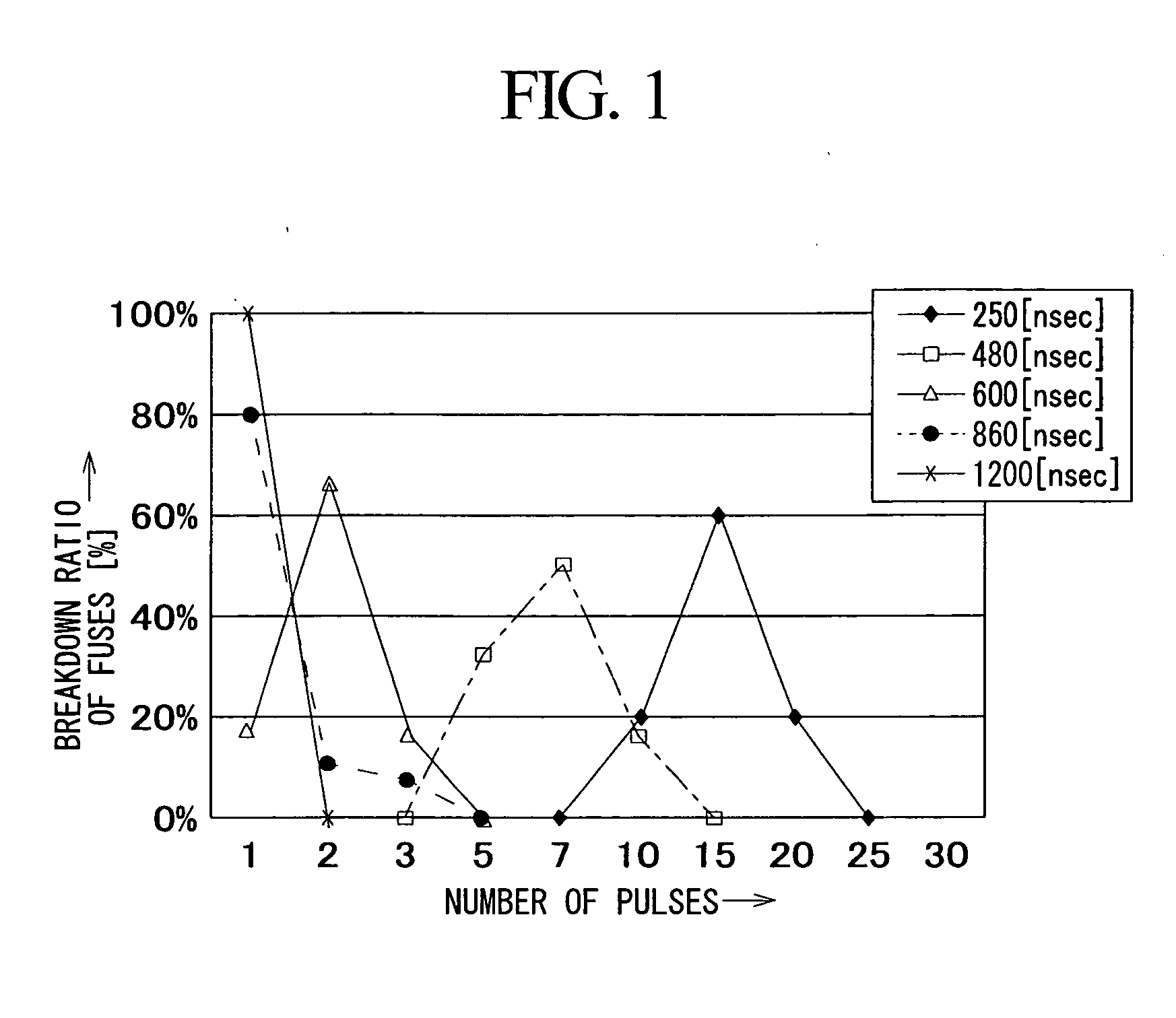
[0240] The aforementioned results may indicate that the method (C), in which the current or voltage is divided by “n”, works well with regard to fuse breakdown. As described above, the energy of a pulse applied to a fuse is reduced by dividing the overall time length, and it is also reduced by dividing the current or voltage.

[0241] The minimum required energy reliably causing breakdown is set to E(1200). This may indicate that each pulse having the energy E(480) may have 1 / 2.5 of the energy E(1200) to be applied to each fuse. The experimental results of FIG. 1 show that each pulse of energy E(480) actually has 1 / 7 of the energy E(1200) because it is weakened due to a decrease of current or voltage; hence, each fuse completely breaks down with multiple pulses each having low energy. Similarly, it is calculated that each pulse having the energy E(250) may have 1 / 4.8 of the energy E(1200); in actuality, however, each pulse of energy E(250) has 1 / 15 of the energy E(1200) b...


PUM


Abstract

A plurality of pulses each having relatively low energy are consecutively applied to a subject fuse to cause breakdown, wherein the total energy of pulses is set in light of a prescribed breakdown threshold, which is calculated in advance. The subject fuse has a pair of terminals and an interconnection portion that is narrowly constricted in the middle so as to realize fuse breakdown with ease. A pulse generator generates pulses, which are repeatedly applied to the subject fuse by way of a transistor; then, it stops generating pulses upon detection of fuse breakdown. Side wall spacers are formed on side walls of fuses, which are processed in a tapered shape so as to reduce thermal stress applied to coating insulating films. In addition, pulse energy is appropriately determined so as to cause electro-migration in the subject fuse, which is thus increased in resistance without causing instantaneous meltdown or evaporation.

Description

BACKGROUND OF THE INVENTION [0001] 1. Field of the Invention [0002] This invention relates to fuse breakdown methods using electric pulses applied to fuses incorporated in semiconductor devices. [0003] The present application claims priority on Japanese Patent Application Nos. 2005-99404, 2005-101481, and 2005-103642, the contents of which are incorporated herein by reference. [0004] 2. Description of the Related Art [0005] Relatively high power, which is higher than the operational power normally applied to electronic circuits, is needed to cause breakdown of fuses formed on semiconductor substrates. For example, MOSFETs are connected in series to fuses so as to cause high currents, causing meltdown and breakdown of fuses, wherein they must have large gate widths, which are several tens of times to several hundreds of times larger than conventional gate widths adapted to MOSFETs generally used for digital processing. However, MOSFETs having large gate widths increase the overall si...

Claims


Application Information

Patent Timeline
Patent Type & Authority Applications(United States)
IPC IPC(8): H01L29/00H01L21/82
CPCH01L23/5256H01L27/112H01L27/11206H01L2924/0002H01L2924/3011H01L2924/00H10B20/00H10B20/20
Inventor OMURA, MASAYOSHISEKIMOTO, YASUHIKO
Owner YAMAHA CORP
Why Eureka
Try Eureka