Detection device and electronic apparatus
A detection device and detection line technology, applied in radiation control devices, circuits, electrical components, etc., can solve the problems of deterioration of transistor characteristics, increase of characteristic differences, signal delay, etc.
- Summary
- Abstract
- Description
- Claims
- Application Information
AI Technical Summary
Problems solved by technology
Method used
Image

Examples
no. 1 Embodiment approach
[0084] (A. Structure and operation of circuit)
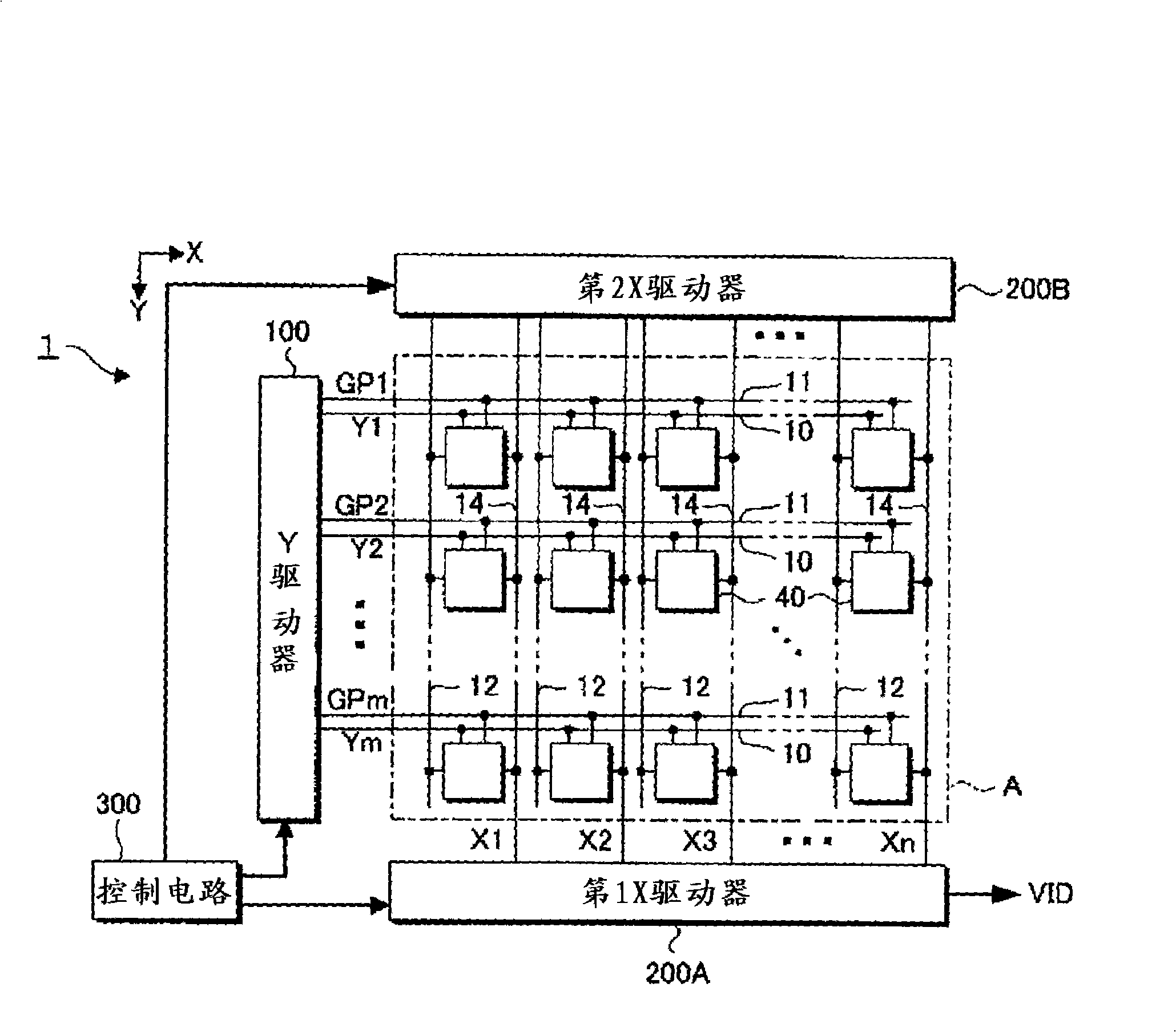
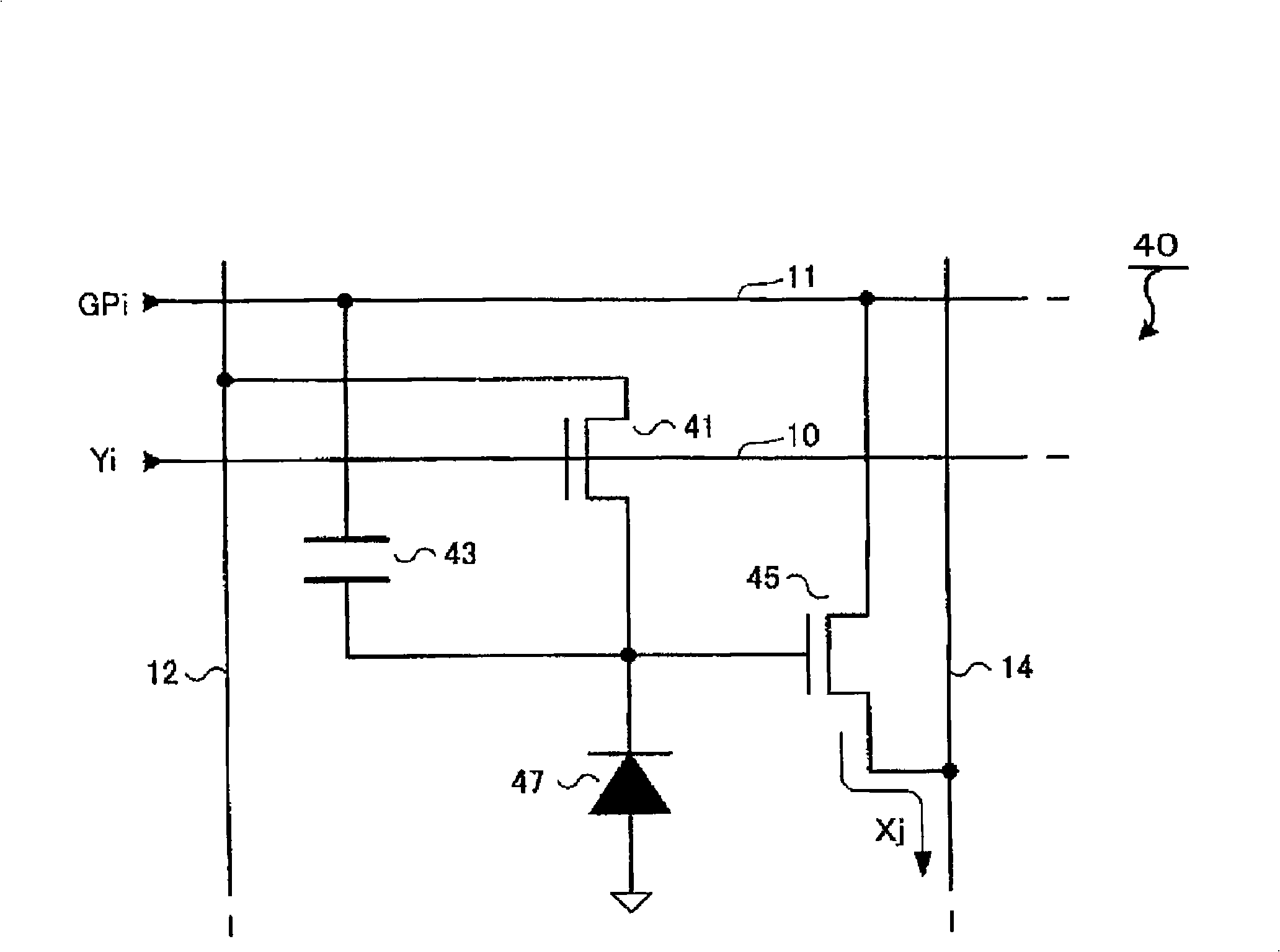
[0085] figure 1 The structure of the detection device of the first embodiment is shown. As shown in the figure, the detection device 1 has a pixel area A, a Y driver 100 , a first X driver 200A, a second X driver 200B, and a control circuit 300 . Among them, in the pixel area A, m scanning lines 10 extending in the X direction, m first power supply lines 11 extending in the X direction in pairs with each scanning line 10, and a line perpendicular to the X direction are formed. There are n second power supply lines 12 extending in the Y direction, and n detection lines 14 extending in the Y direction in pairs with the second power supply lines 12 . Pixel circuits 40 (unit circuits) are arranged at positions corresponding to intersections of the scanning lines 10 and the second power supply lines 12 . Therefore, these pixel circuits 40 are arranged in a matrix of m rows x n columns.
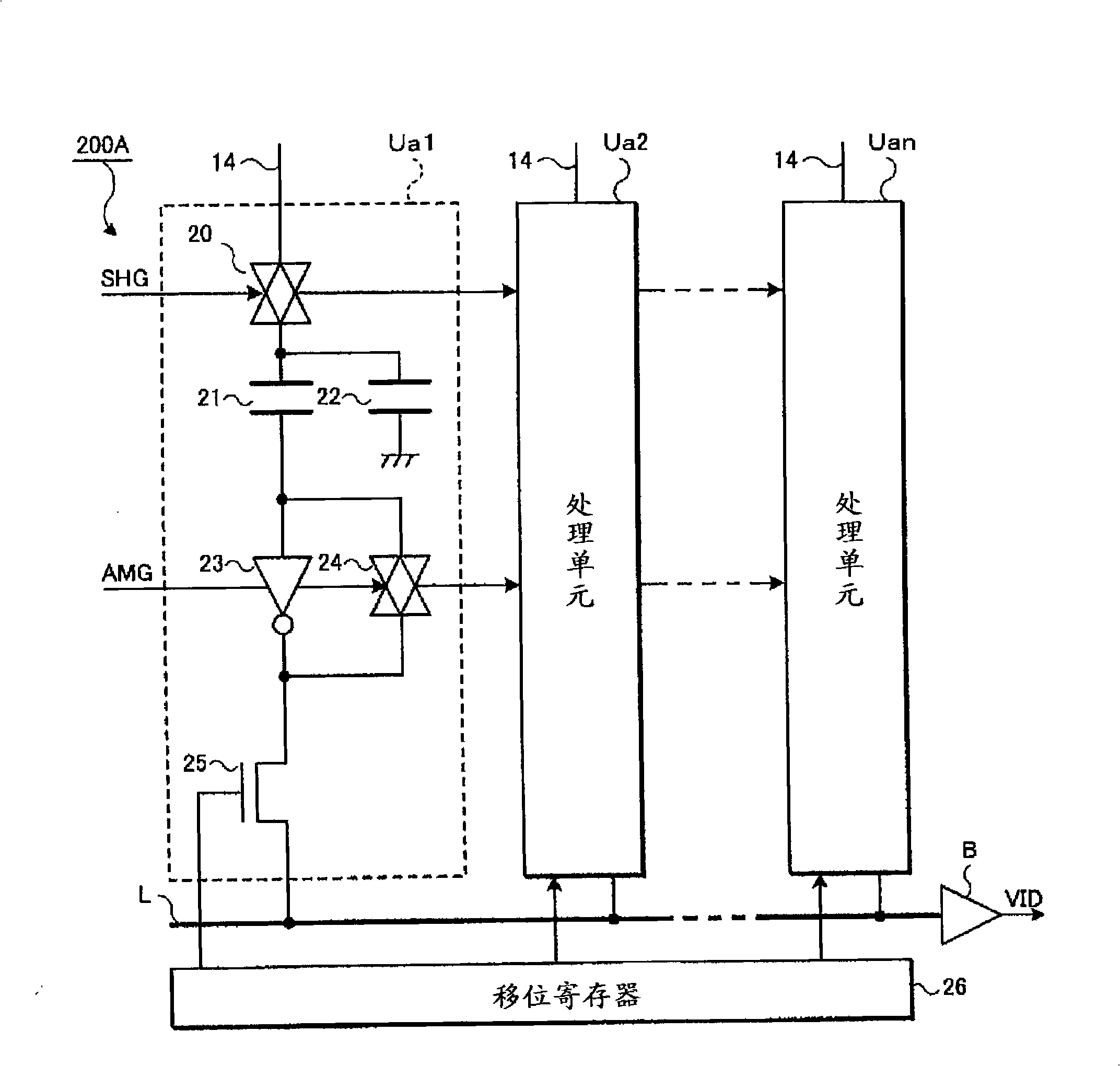
[0086] The Y driver 100 selects each of th...
Deformed example 1-1
[0125] The detection device 1 of the present embodiment uses the photodiode 47 as a detection element, but other various detection elements may be used instead. Figure 21 It is a cross-sectional view of the detection device 1 using the second capacitive element 44 as a detection element, and the position of the cross-section corresponds to the position of the line B-B in FIG. 11 . The second capacitive element 44 is formed overlapping the first capacitive element 43, and has a structure in which the first electrode 43a, the insulating layer 44d, and the second electrode 44b are layered from the lower layer. Here, the first electrode 43 a is an electrode shared with the first capacitive element 43 . A substrate 6 made of glass, transparent resin, or the like is arranged on the upper surface of the second capacitive element 44 . When the substrate 6 is deformed due to external factors, the thickness of the insulating layer 44d changes, thereby changing the capacitance of the s...
Deformed example 1-2
[0127] The detection device 1 of this embodiment has two power supply lines (the first power supply line 11 and the second power supply line 12) in each pixel circuit 40, but these power supply lines may be shared by electrically connecting them, and each The pixel circuit 40 has a structure of a single power supply line. Figure 22 It is a circuit diagram of the detection device 1 having the pixel circuit 40 configured in this way. In each pixel circuit 40 , one terminal of the first capacitive element 43 is electrically connected to the second power supply line 12 (also simply referred to as the power supply line 12 in this modified example). Also, one terminal (source or drain) of the reset transistor 41 and the amplification transistor 45 is both electrically connected to the power supply line 12 . In this way, the power supply voltage RSL can be supplied to the terminal of the first capacitive element 43 and one end of the reset transistor 41 and the amplification transi...
PUM
 Abstract
Description
Claims
Application Information
 - R&D
- Intellectual Property
- Life Sciences
- Materials
- Tech Scout
- Unparalleled Data Quality
- Higher Quality Content
- 60% Fewer Hallucinations
Browse by: Latest US Patents, China's latest patents, Technical Efficacy Thesaurus, Application Domain, Technology Topic, Popular Technical Reports.
© 2025 PatSnap. All rights reserved.Legal|Privacy policy|Modern Slavery Act Transparency Statement|Sitemap|About US| Contact US: help@patsnap.com