

Display device
A technology for display devices and potentials, applied in static indicators, logic circuit connection/interface layout, logic circuit coupling/interface using field effect transistors, etc., can solve problems such as difficult to simplify the circuit composition of display devices
- Summary
- Abstract
- Description
- Claims
- Application Information
AI Technical Summary
Problems solved by technology
Method used
Image

Examples
no. 1 Embodiment
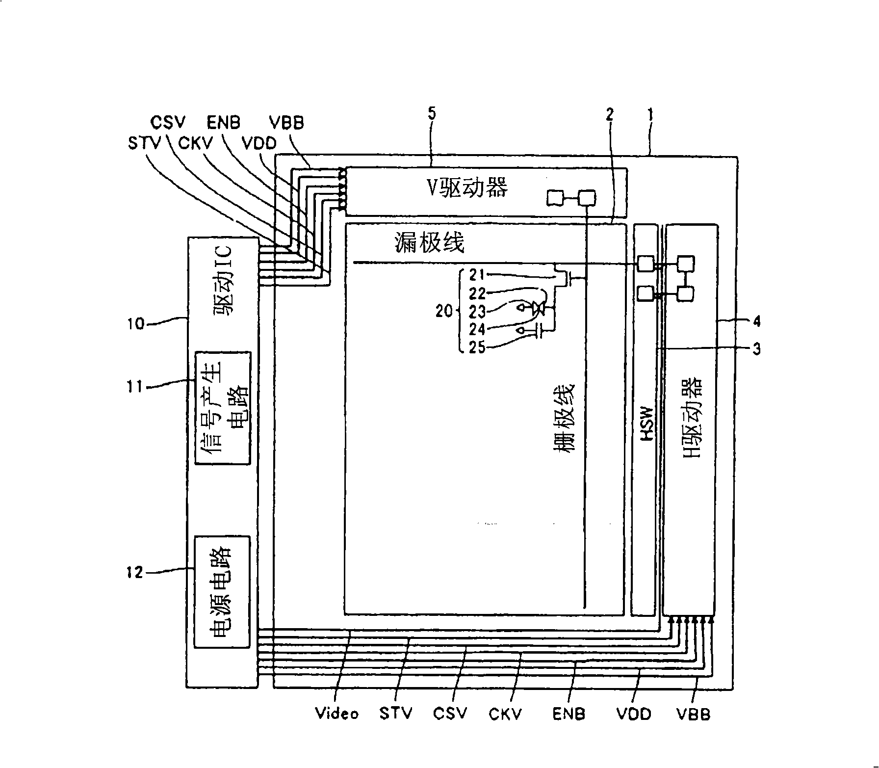
[0112] First refer to figure 1 , in this first embodiment, the display portion 2 is provided on the substrate 1 . In the display unit 2 , pixels 20 are arranged in a matrix. exist figure 1 In , only one pixel 20 is shown in order to simplify the drawing. Each pixel 20 is composed of: an n-channel transistor 21 (hereinafter referred to as a transistor 21), a pixel electrode 22, an opposite electrode 23 common to each pixel 20 arranged opposite to the pixel electrode 22, and surrounded by the pixel electrode 22 and the opposite electrode. The liquid crystal 24 between the electrodes 23 and the storage capacitor 25 constitute. The source of the transistor 21 is connected to the pixel electrode 22 and the storage capacitor 25 , and the drain is connected to the drain line. The gate of this transistor 21 is connected to a gate line.
[0113] Further, a horizontal switch (HSW) 3 and an H driver 4 for driving (scanning) a drain line of the display unit 2 are provided on the su...
no. 2 Embodiment
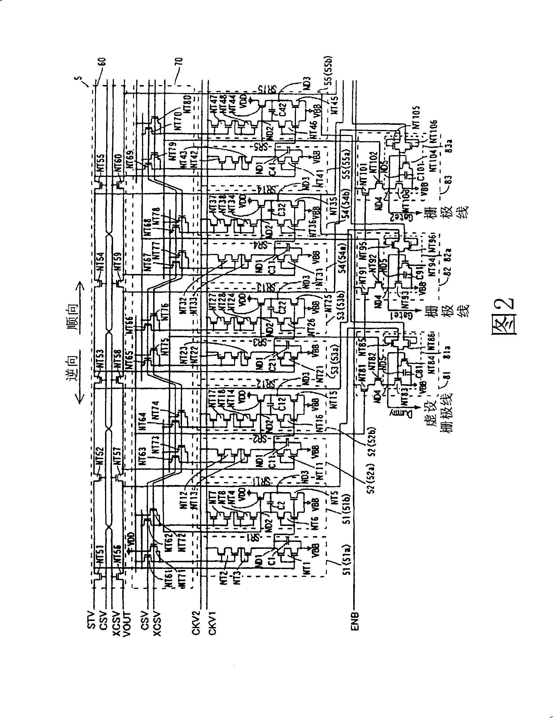
[0204] The second embodiment has almost the same configuration as the first embodiment. Referring to Fig. 5, the difference from the first embodiment is that in the inside of the V driver 5a, shift register circuit sections 501 to 505, a scanning direction switching circuit section 600, an input signal switching circuit section 700, And the transistors of the multi-stage logic synthesis circuit sections 801 to 803 are changed to p-channel transistors. In FIG. 5, in order to simplify the drawing, only 5 stages of shift register circuit sections 501 to 505 and 3 stages of logic synthesis circuit sections 801 to 803 are shown, but in fact shift register circuits corresponding to the number of pixels are arranged. Bit register circuit section and logic synthesis circuit section.
[0205] Next, the operation of the V driver 5a of the liquid crystal display device of the second embodiment will be described with reference to FIGS. 5 and 6. FIG. In the V driver 5a of the second embo...
no. 3 Embodiment
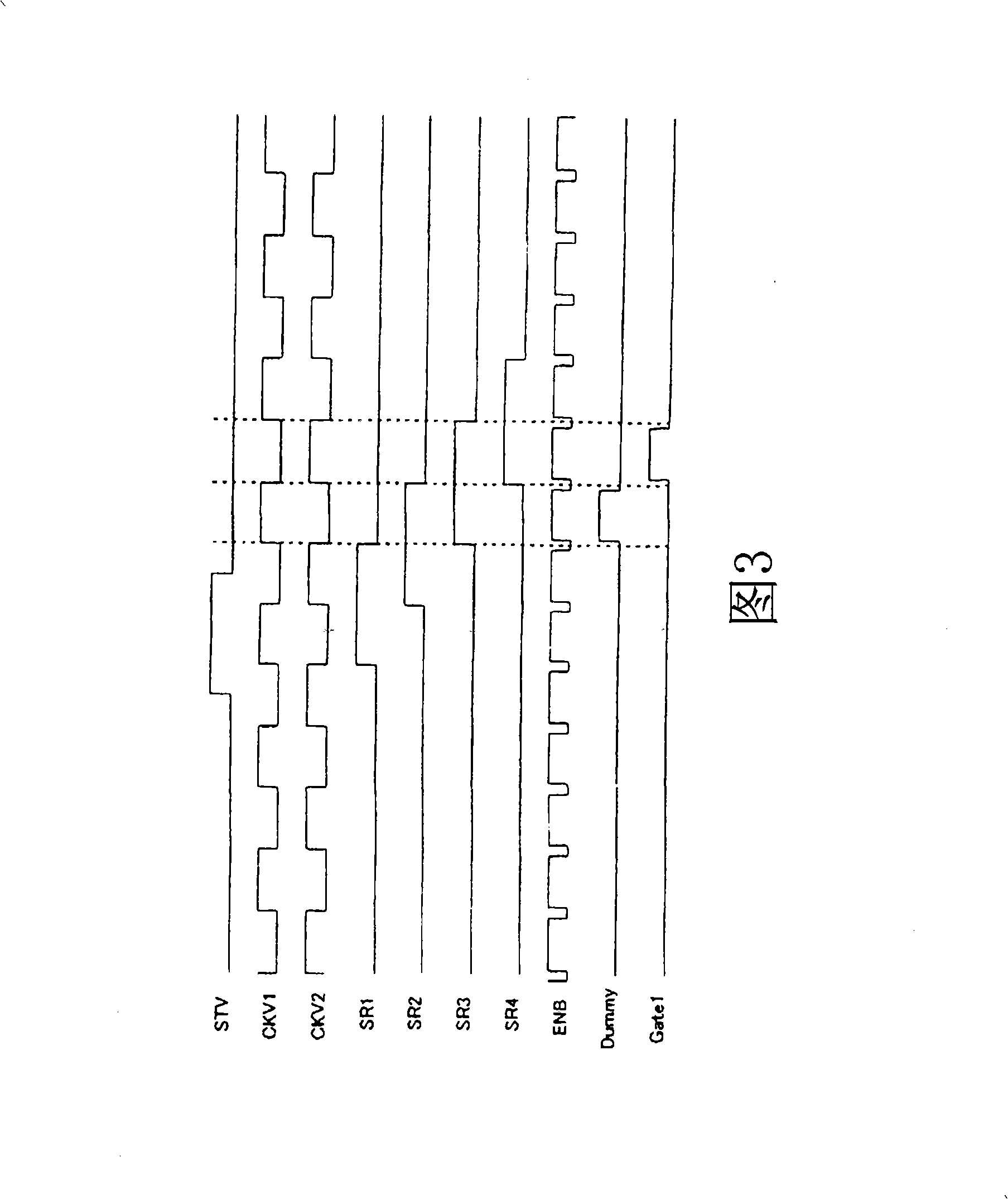
[0208] Referring to FIG. 7, in the third embodiment, in the configuration of the above-mentioned first embodiment, the drain of the transistor connected to the node of the shift register circuit section after the third stage is output with a shift output signal, A case where an enable signal is supplied instead of the positive side potential.
[0209] That is, as shown in FIG. 7, in this third embodiment, multistage shift register circuit sections 511 to 515, scanning direction switching circuit section 610, input signal switching circuit section 710, and multistage logic synthesis circuit section are provided. 811 to 813. In FIG. 7, in order to simplify the drawing, only 5 stages of shift register circuit sections 511 to 515 and 3 stages of logic synthesis circuit sections 811 to 813 are shown, but in fact, shift registers corresponding to the number of pixels are arranged. A register circuit unit and a logic synthesis circuit unit.
[0210] In addition, the shift register ...
PUM
 Abstract
Description
Claims
Application Information