Photovoltaic cell

A photovoltaic cell and semiconductor technology, applied in circuits, electrical components, semiconductor devices, etc., can solve the problems of expensive device manufacturing costs, achieve the effects of improving efficiency, saving exchange time, and avoiding room condition adjustment

Inactive Publication Date: 2008-12-31
HELIANTHOS BV
View PDF2 Cites 18 Cited by
  • Summary
  • Abstract
  • Description
  • Claims
  • Application Information

AI Technical Summary

Problems solved by technology

[0006] The problem with the latter cell is that in order to be sufficiently effective it must comprise a very large number of combinations of layers of different semiconductor materials forming the active region
However, adding additional layers to the superlattice would make known devices expensive to manufacture

Method used


Image

  • Photovoltaic cell
  • Photovoltaic cell
  • Photovoltaic cell

Examples


Embodiment Construction

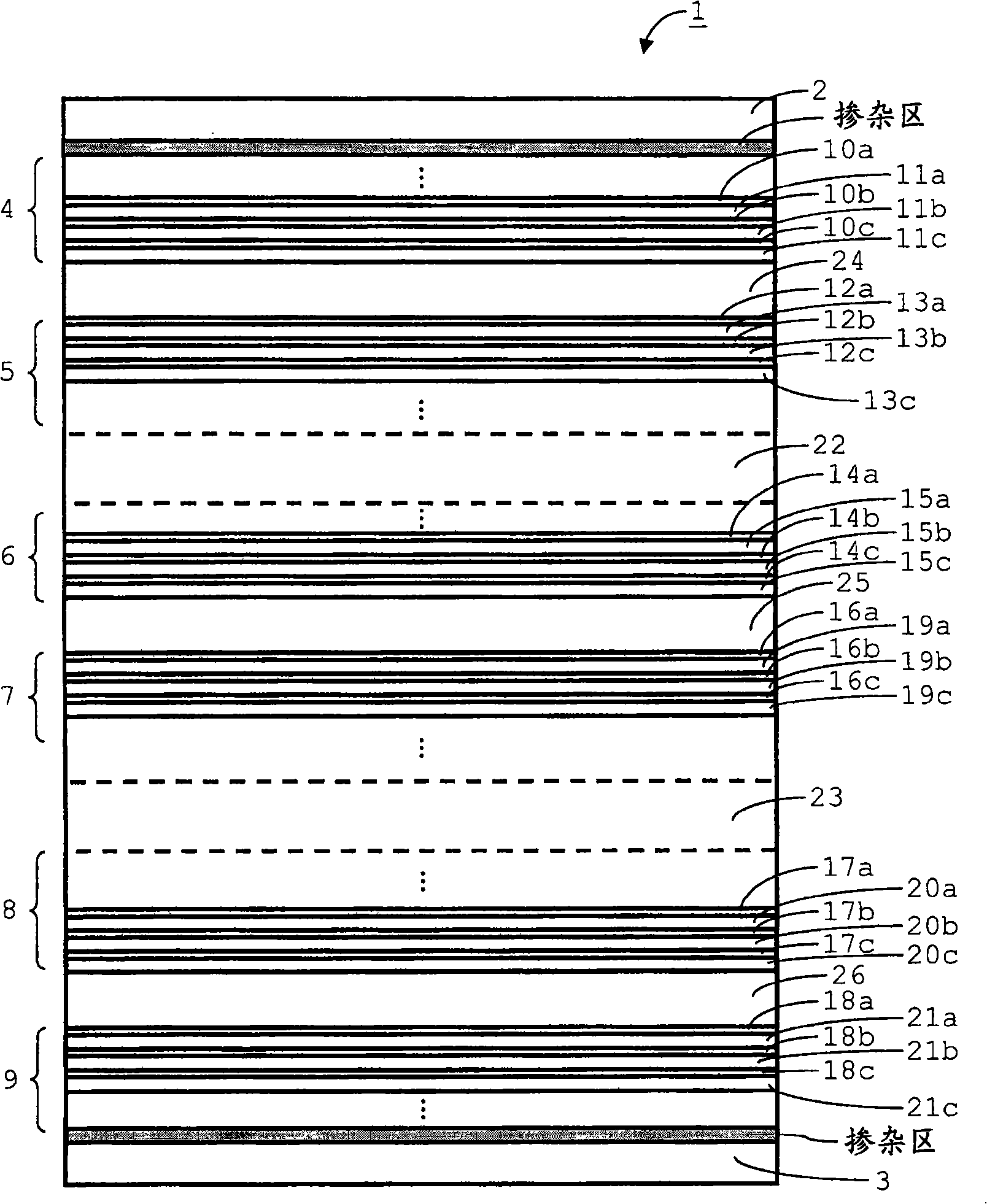
[0035] figure 1 The photovoltaic cell 1 is shown only to the extent necessary to illustrate the present invention. In a practical photovoltaic device, the photovoltaic cell 1 will be encased in other layers including one or more layers of plastic foil and / or glass sheets for isolating the photovoltaic cell from the environment. In the illustrated embodiment, the photovoltaic cell 1 is a tandem cell, ie a stack of component cells. In this case, the individual cells in the stack are electrically connected in series. Paralleling is an alternative, but more complicated.

[0036] The illustrated photovoltaic cell 1 is a two-terminal device and comprises a top electrode 2 and a back electrode 3 . The top electrode is made of transparent conductive material such as SnO 2 (tin oxide), ITO (indium tin oxide), ZnO (zinc oxide), Zn 2 SnO 4 (zinc stannate), Cd 2 SnO 4(cadmium stannate) or InTiO (indium titanium oxide). The back electrode 3 is at least partially made of a metal su...


PUM


Abstract

The invention relates to a photovoltaic cell, including at least a first junction between a pair of semiconducting regions (4-9) . At least one of the pair of semiconducting regions includes at least part of a superlattice comprising a first material interspersed with formations of a second material. The formations are of sufficiently small dimensions so that the effective band gap of the superlattice is at least partly determined by the dimensions. An absorption layer (24-26) is provided between the semiconducting regions and the absorption layer comprises a material for absorption of radiation so as to result in excitation of charge carriers and is of such thickness that excitation levels are determined by the material itself . At least one of the effective energy bands of the superlattice and one of the excitation levels of the material of the absorption layer is selected to match at least one of the excitation levels of the material of the absorption layer and the effective energy band of the superlattice, respectively.

Description

technical field [0001] The invention relates to a photovoltaic cell comprising at least a first junction between a pair of semiconductor regions, wherein at least one of the pair of semiconductor regions comprises at least part of a superlattice comprising a formation with a second material Alternating the first material, the formation has a size small enough that the effective bandgap of the superlattice is determined at least in part by the size, wherein the absorbing layer is disposed between the semiconductor regions, and wherein the absorbing layer includes a The absorbing material so as to cause excitation of carriers, and the absorbing layer has such a thickness that the excitation energy level is determined by the material itself. [0002] The invention also relates to a method of manufacturing a photovoltaic cell array. [0003] The invention also relates to a photovoltaic device comprising a plurality of photovoltaic cells. Background technique [0004] Examples ...

Claims


Application Information

Patent Timeline
Patent Type & Authority Applications(China)
IPC IPC(8): H01L31/0352
CPCH01L31/035245
Inventor M·泽曼G·J·约恩格登
Owner HELIANTHOS BV
Why Eureka
Try Eureka