Photo-etching method

A technology of photolithography and photoresist, which is applied in the direction of optics, optomechanical equipment, instruments, etc., can solve the problems of inability to etch graphics to meet the requirements, poor uniformity of key dimensions of graphics, etc., and achieve the effect of good control consistency and uniformity

Inactive Publication Date: 2009-01-14
GRACE SEMICON MFG CORP
View PDF0 Cites 11 Cited by
  • Summary
  • Abstract
  • Description
  • Claims
  • Application Information

AI Technical Summary

Problems solved by technology

However, inspection after the etch step found that the graphic critical dimension uniformity is poor, such as image 3 As shown, the pattern CD variation in the center part of the wafer is smaller than that in the edge part
Using the existing method, the etching pattern and the required circuit pattern are quite different, and because the pattern distortion is different at different positions on the wafer, the traditional method such as optical approach correction and exposure machine approach correction is due to its The limitation of itself cannot make the etching pattern meet the requirements

Method used


Image

  • Photo-etching method
  • Photo-etching method
  • Photo-etching method

Examples


Embodiment Construction

[0016] The photolithography method disclosed in the present invention will be further described in detail below in conjunction with the accompanying drawings.

[0017] see Figure 4 to Figure 6 , the photolithography method of the present invention comprises the following steps:

[0018] Provide wafers to be processed;

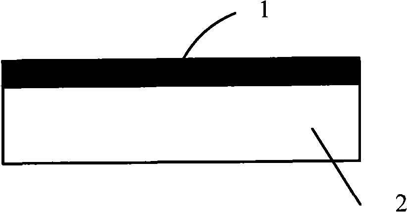
[0019] Coating photoresist 4 on the surface of the etched layer 3 of the wafer, the thickness of the photoresist 4 gradually increases uniformly from the center of the wafer to the periphery;

[0020] performing an exposure step;

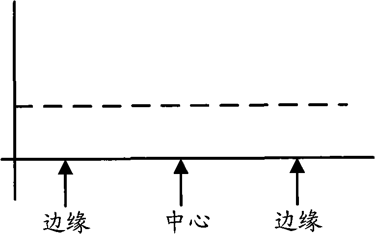
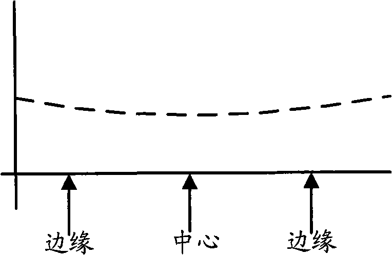
[0021] Carry out the development step, and detect and find after the development step, the graphic key dimension consistency curve, such as Figure 5 As shown, the shape of the graph is consistent with the shape of the photoresist thickness;

[0022] Perform the etching step to form the required circuit pattern on the etched layer 3. After inspection, it is found that the key dimensions of the pattern at each position of the waf...


PUM


Abstract

The invention discloses a lithography method, relating to the semiconductor manufacturing field and aiming at overcoming the defect of the traditional lithography method that the evenness of etched patterns is poor. The lithography method of the invention includes the following steps: a wafer to be processed is provided; photoresist is plated on the surface of an etched layer of the wafer and the thickness of the photoresist at the center of the wafer is different from that of the peripheral parts of the wafer; an exposure step is carried out; a development step is carried out; an etching step is carried out; and the remaining photoresist is removed. Compared with the prior art, the method can obtain a circuit pattern with better evenness and the unification for the etched patterns can be further controlled for the distortion states of position patterns on the wafer are identical and then the traditional methods such as the correction methods of optical approaching correction and exposure machine approaching correction, etc., can be conveniently adopted.

Description

technical field [0001] The invention relates to manufacturing technology in the field of semiconductors, in particular to a photolithography method for semiconductor devices. Background technique [0002] With the rapid development of semiconductor technology, semiconductor devices are becoming more and more sophisticated, which makes it more difficult for people to control process errors. The lithography process is an important link in the manufacture of semiconductor devices, and how to obtain a better critical dimension (CD) in the lithography process is becoming more and more important. [0003] The existing method of etching pattern is: at first at first the etched layer 1 surface of wafer is plated photoresist 2, and photoresist thickness is uniform, as figure 1 Shown; Then carry out developing step, if what adopt positive photoresist, then the photoresist of exposure area is removed; Then carry out etching step, etch out required circuit pattern on etched layer 2; p...

Claims


Application Information

Patent Timeline
Patent Type & Authority Applications(China)
IPC IPC(8): G03F7/00G03F7/16H01L21/027
Inventor 周孟兴
Owner GRACE SEMICON MFG CORP
Why Eureka
Try Eureka