Repairing line structure and method for manufacturing same

A technology for repairing lines and scanning lines, which is applied in nonlinear optics, instruments, optics, etc., and can solve problems such as existence, increasing coupling capacitance, and affecting the normal repair of repair lines.

Inactive Publication Date: 2009-02-04
SHANGHAI SVA LIQUID CRYSTAL DISPLAY
View PDF0 Cites 6 Cited by
  • Summary
  • Abstract
  • Description
  • Claims
  • Application Information

AI Technical Summary

Problems solved by technology

[0006] Since there are a large number of signal scanning lines in the display area, and there are a large number of overlapping points directly with the repairing lines, during the repairing process, other undotted signal scanning lines and the overlapping points of the repairing lines will generate coupling capacitance along with the signal scanning. The increase of the line keeps getting bigger, and the coupling capacitance between the repair line and the target liquid crystal electrode and the resistance of the repair line itself exist, thus affecting the normal repair of the repair line

Method used


Image

  • Repairing line structure and method for manufacturing same
  • Repairing line structure and method for manufacturing same
  • Repairing line structure and method for manufacturing same

Examples


Embodiment 1

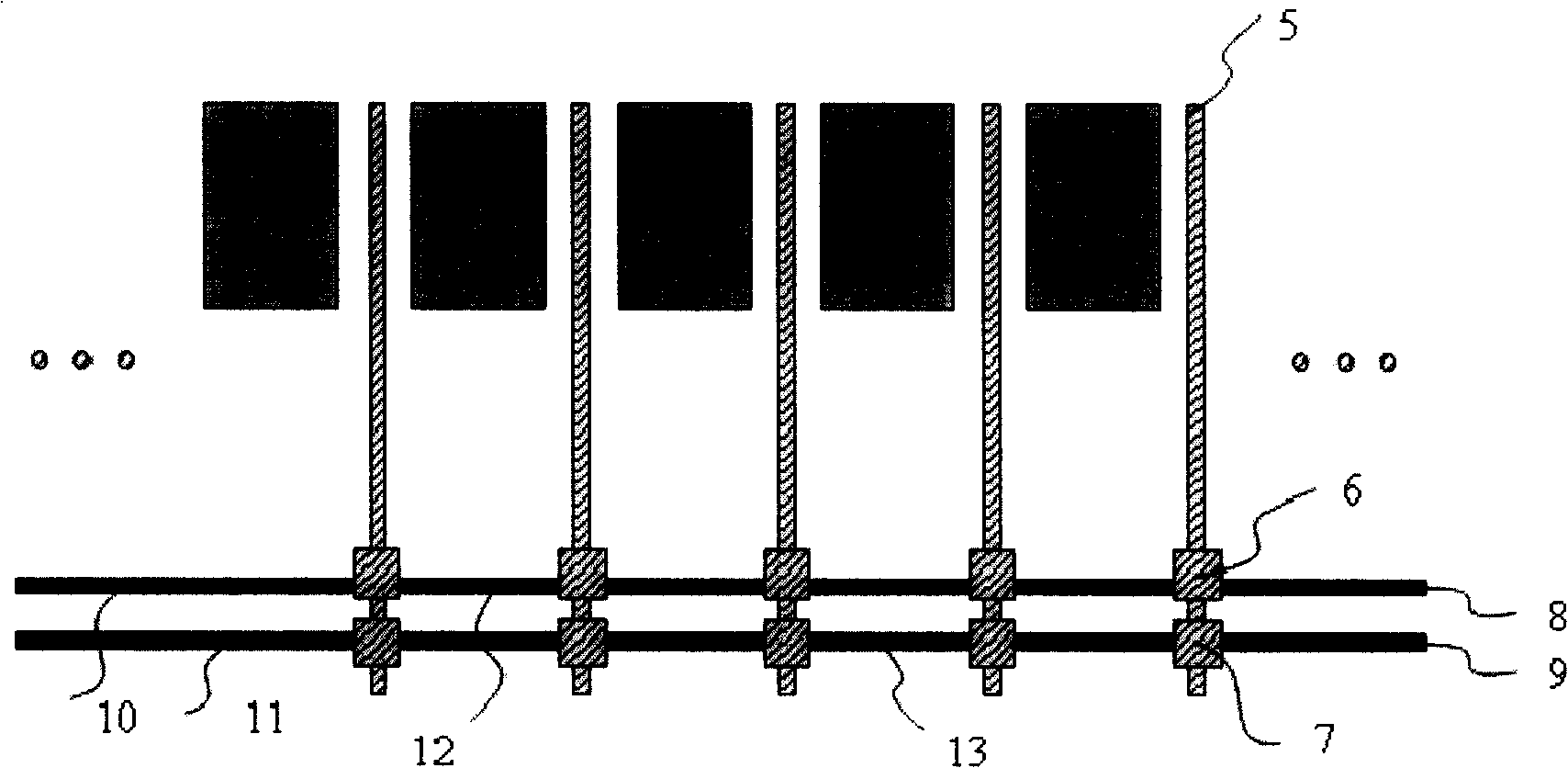
[0030] like Figure 5 , intermittent repair line 3, auxiliary repair line 4 is the same layer process, the same layer of metal sputtering manufacturing; repair line, signal scanning line is the same layer process, the same layer of metal sputtering manufacturing; repair lines L1, L2 and intermittent repair Line 3 is made by non-same-layer process and non-same-layer metal sputtering.

[0031] When repairing one point, the repairing signal can be input from any point of 14 and 15; when repairing two points, the repairing signal can be input from two points of 14 and 15. When repairing more than two points, the number of 12, 13 repair lines and repair signal input lines can be increased accordingly, and the number of intermittent repair lines can be two or more rows.

[0032] When the scanning signal line 5 needs to be repaired, you can connect the repair points 2 and 6 by laser dotting, or do the following points by laser marking: 1, 6 methods; 2, 7 methods; 1, 7 methods; 2, 17...

Embodiment 2

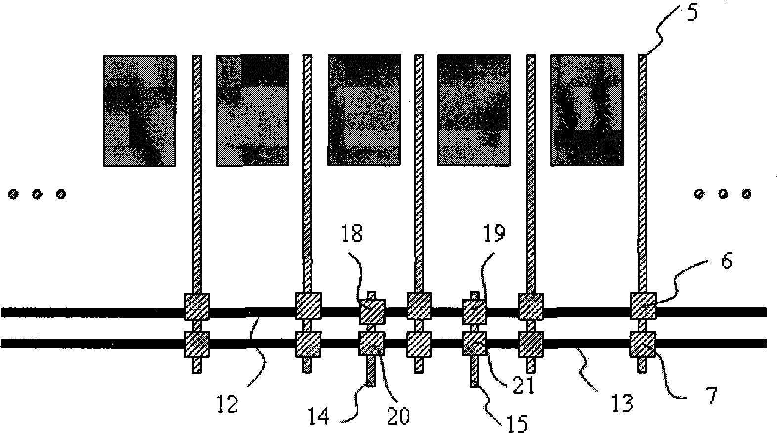
[0039] like Image 6 , intermittent repair line 3, auxiliary repair line 4 is the same layer process, the same layer of metal sputtering manufacturing; repairing lines L1, L2 and scanning signal line 5 are the same layer process, the same layer of metal sputtering manufacturing; repairing lines L1, L2 , The intermittent repair line is made by non-same-layer technology and non-same-layer metal sputtering.

[0040] When repairing one point, the repair signal can be input from any point among 8, 9, 10, 11; when repairing two points, the repair signal can be input from any two points among 8, 9, 10, 11; when repairing more than two points, The number of 12, 13 repair lines and repair signal input lines can be increased accordingly, and the number of intermittent repair lines can be two or more rows.

[0041] When the scanning signal line 5 needs to be repaired, the repair points 2 and 6 can be connected by laser dotting, or the following laser dotting methods can be used: 1, 6, 2...

Embodiment 3

[0044] like Figure 7 , the intermittent repair line 3, the auxiliary repair line 4 is manufactured by a different layer process, and the metal sputtering is not the same layer; the repair lines L1, L2 and the signal scanning line 5 are not made by the same layer process, and the metal sputtering is not made by the same layer; Lines L1, L2, and discontinuous repair lines are manufactured by the same layer process and metal sputtering on the same layer.

[0045] When repairing one point, the repair signal can be input from any point of 14 and 15; when repairing two points, the repair signal can be input from two points 14 and 15; when repairing more than two points, the repair line of 12 and 13 and the repair signal can be added accordingly Enter the number of lines, and the number of intermittent repair lines can be two rows or more.

[0046]When the scanning signal line 5 needs to be repaired, you can connect the repair points 2 and 6 through laser dots, or you can use 1 and...


PUM


Abstract

The invention provides a new repairing line structure, which comprises the original repairing lines, intermittent repairing lines and auxiliary repairing lines; the repairing lines are not directly overlapped with signal scan lines. The intermittent repairing lines are partially overlapped with two signal scan lines, or more than two signal scan lines are outspread as a unit. The intermittent repairing lines and the signal scan lines are overlapped into two or more rows. The manufacturing method of the repairing line structure is as follows: a metal film is arranged on a substrate through sputtering; a mask template forms intermittent repairing lines and auxiliary repairing lines outside a pixel area of the substrate through the exposure process and the chemical etching process; an electrode insulating layer film is arranged on the substrate; a metal film is deposited on the substrate; the mask template forms array substrate signal scanning electrodes through the exposure process and the chemical etching process, and forms the repairing lines outside the pixel area of the substrate at the same time. The repairing points are completely positioned in liquid crystal so as to avoid bad connections caused by oxidation corrosion; in addition, various repairing routes are provided to avoid incapable repairing due to the breaking of certain repairing line. The repairing points are completely positioned in liquid crystal so as to avoid bad connections caused by oxidation corrosion; in addition, various repairing routes are provided to avoid incapable repairing caused by the breaking of certain repairing line.

Description

technical field [0001] The invention relates to the field of liquid crystal display (TFT LCD), in particular to a repair line structure and a manufacturing method of a thin film transistor liquid crystal display. Background technique [0002] Liquid crystal display is a kind of passive display. It cannot emit light by itself and can only use the light of the surrounding environment. Since the liquid crystal display only needs a small amount of energy to display patterns or characters, it makes LCD a better display method. The liquid crystal material used in liquid crystal display is an organic substance with both liquid and solid properties. Its rod-like structure is arranged in the liquid crystal cell, but its alignment direction can be changed under the action of an electric field. [0003] Generally, a liquid crystal display device has two upper and lower substrates 20 spaced apart from each other and facing each other. A plurality of electrodes formed on the two substra...

Claims


Application Information

Patent Timeline
Patent Type & Authority Applications(China)
IPC IPC(8): G02F1/13
Inventor 李小和
Owner SHANGHAI SVA LIQUID CRYSTAL DISPLAY
Why Eureka
Try Eureka