Substrate outer appearance inspection device

A technology for visual inspection devices and substrates, which is applied to measuring devices, optical devices, and material analysis through optical means, and can solve problems such as difficulty in dealing with substrates with high components, inability to cope with substrates, and miniaturization of components.

Active Publication Date: 2009-02-11
ORMON CORP
View PDF2 Cites 41 Cited by
  • Summary
  • Abstract
  • Description
  • Claims
  • Application Information

AI Technical Summary

Problems solved by technology

[0013] However, in the lighting device of the color high-intensity method, since it illuminates in all directions, in order to increase the irradiation range, the width must be increased in all directions, resulting in an increase in the size of the lighting device, and it cannot cope with the current situation of miniaturization of the substrate and parts.
In addition, if the lighting part is lowered, it is difficult to cope with the substrate on which tall components are mounted.

Method used


Image

  • Substrate outer appearance inspection device
  • Substrate outer appearance inspection device
  • Substrate outer appearance inspection device

Examples


Embodiment Construction

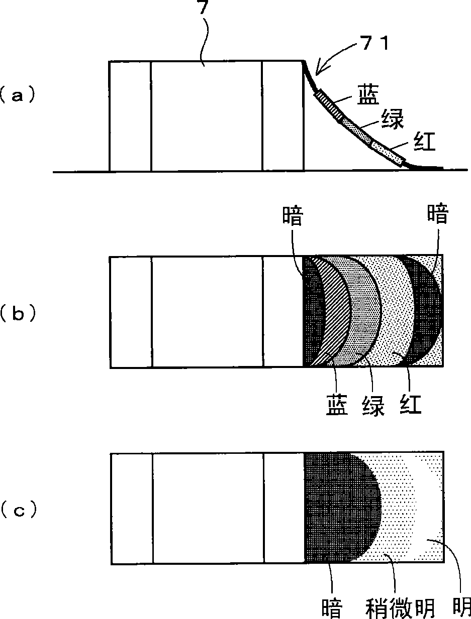
[0039] Next, an example of a substrate visual inspection device that inspects a substrate after a series of processes (solder printing process, component mounting process, and soldering process) for manufacturing a component-mounted substrate and inspects the appearance of each component will be described. Whether the installation state and the shape of the solder fillet are appropriate.

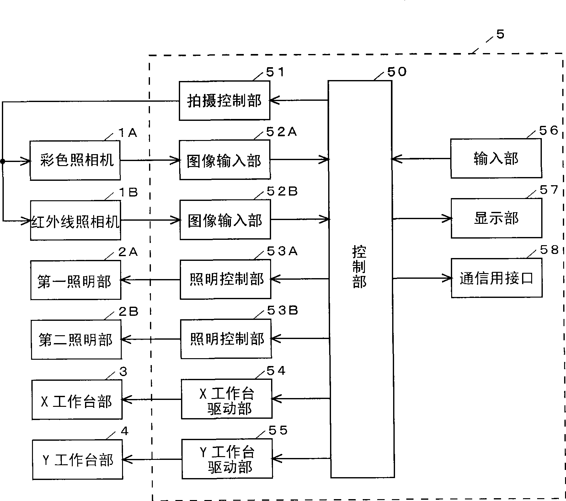
[0040] figure 1 It is a block diagram showing an example of the electrical configuration of the substrate appearance inspection device of this embodiment.

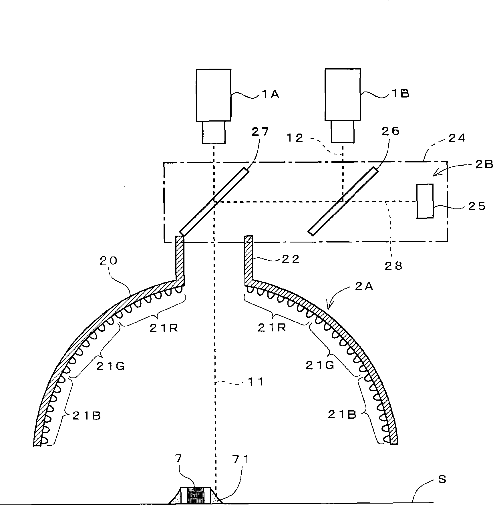
[0041] The inspection device is respectively provided with two cameras 1 and lighting units 2 as devices for generating substrate images of inspection objects (hereinafter, the cameras 1 and the lighting units 2 that have a corresponding relationship are combined, and symbols A and B are used to distinguish each Group). In addition, this inspection device is provided with an X stage unit 3, a Y stage unit 4, a control processing unit ...


PUM


Abstract

The invention provides a substrate appearance inspection device capable of differentiating solder steep surface and plane surface, which are hard to detect out with colorful high-brightness illumination, and capable of picking-up position out of the solder in white illumination. A colorful camera and infrared camera are arranged above a substrate to make each light receiving faces opposite to the substrate face. A first illumination section respectively irradiating visible lights such as red, green, blue from different directions and a second illumination section irradiating infrared light along light axis of the camera are arranged between the camera and substrate. Color image is formed by reflected light reflected by the incidence substrate of the camera from the first illumination section, shade image is formed by reflected light of camera incidence infrared light. Image of position corresponding to the color image is processed when detecting position out of the welded corner, position corresponding tilt grade of five-grade is determined by using color image and shade image when detecting the welded corner.

Description

technical field [0001] The present invention relates to a substrate appearance inspection device that photographs a printed substrate (hereinafter referred to as "parts mounted substrate" or simply "substrate") and uses the generated image to determine the mounting state of components and soldering conditions. Whether the surface condition, etc., of the above-mentioned substrate on which components are mounted and the soldering of each mounted component has been completed is suitable. Background technique [0002] The applicant has developed more substrate appearance inspection devices called "color high light" than ever before. This color high-brightness substrate appearance inspection device (hereinafter simply referred to as "inspection device") has a two-dimensional color camera and an illumination device that emits red, green, and blue color lights from different directions (refer to Patent Document 1, 2). [0003] Patent Document 1: JP Kohei No. 6-1173 [0004] Pate...

Claims


Application Information

Patent Timeline
Patent Type & Authority Applications(China)
IPC IPC(8): G01N21/956G01B11/26G01N21/84
Inventor 栗山淳本冈修泽彩中塚俊介藤井心平
Owner ORMON CORP
Why Eureka
Try Eureka