Colourful filtering substrate, method for manufacturing same and liquid crystal display panel
A technology of color filter substrate and manufacturing method, which is applied in the fields of optics, nonlinear optics, instruments, etc., can solve the problems of large amount of radiation, unsatisfactory, limited space for product flattening, etc., and achieve less process steps and less electrical resistance short circuit effect
- Summary
- Abstract
- Description
- Claims
- Application Information
AI Technical Summary
Problems solved by technology
Method used
Image

Examples
no. 1 example
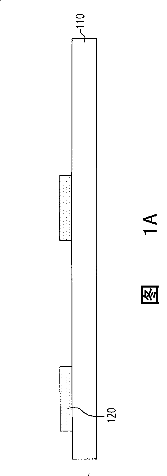
[0025] 1A to 1E are cross-sectional views of a manufacturing method of a color filter substrate according to a first embodiment of the present invention. Please refer to FIG. 1A , the manufacturing method of the color filter substrate of this embodiment includes the following steps. Firstly, a substrate 110 is provided, and a first colored layer 120 is formed on the substrate 110 . Wherein, the material of the first colored layer 120 includes a photoresist material, and the method of forming the first colored layer 120 includes an exposure process and a development process.
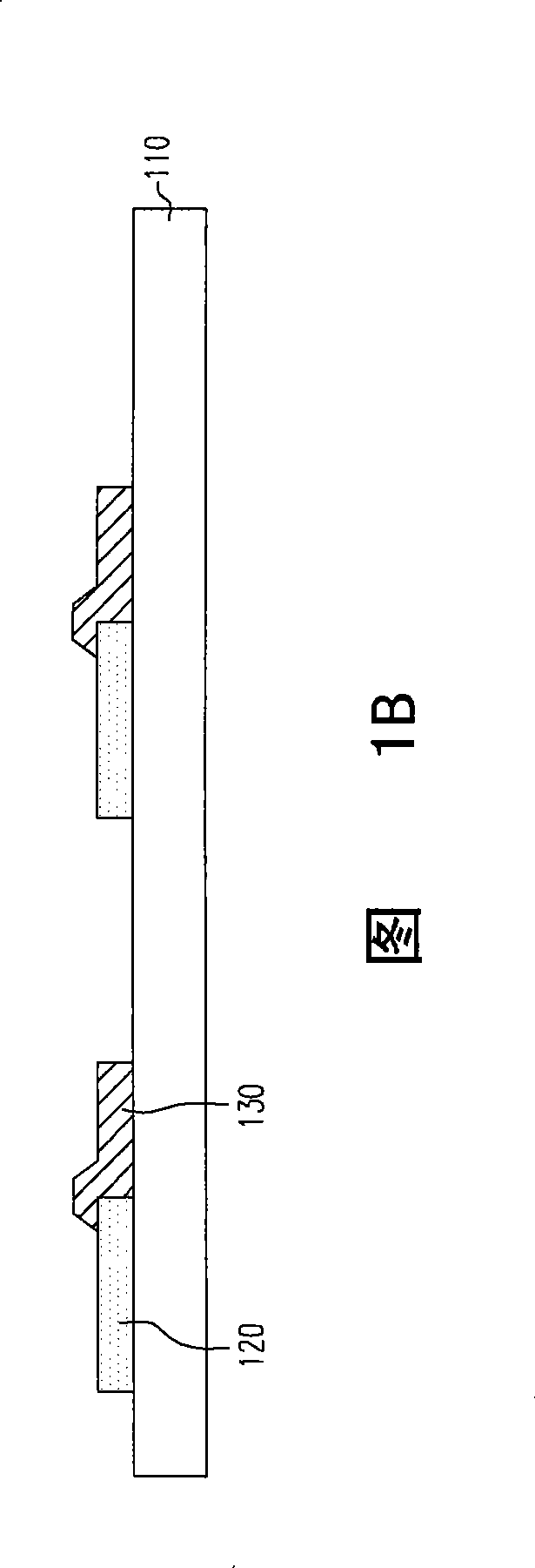
[0026] Referring to FIG. 1B , a second colored layer 130 is formed on the substrate 110 , wherein the second colored layer 130 partially overlaps with the first colored layer 120 . In addition, the method of forming the second color layer 130 is the same as the method of forming the first color layer 120 .
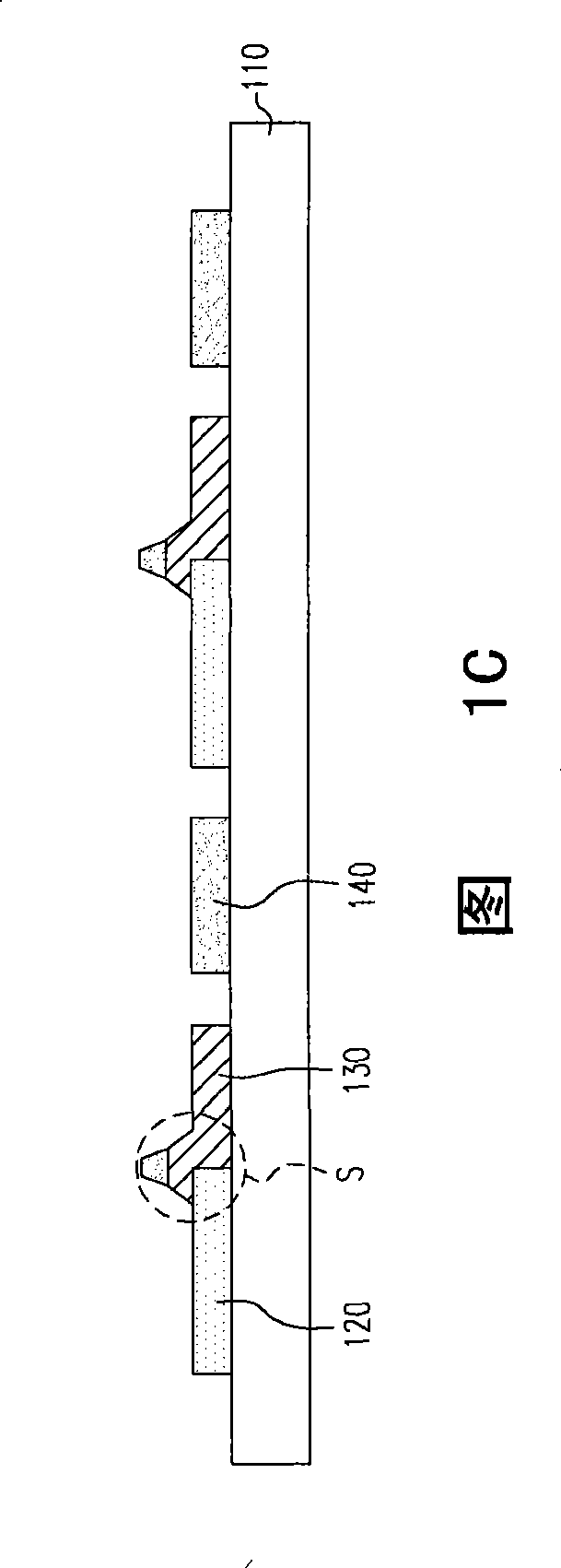
[0027] Referring to FIG. 1C , a third colored layer 140 is formed on the substrate 110 , and par...
no. 2 example
[0036] FIG. 3 is a cross-sectional view of a color filter substrate according to a second embodiment of the present invention. Please refer to FIG. 3 , this embodiment is similar to the first embodiment, the difference is that: when the light shielding layer 160 is not accurately formed on the common electrode layer 150 above the support S, the light shielding layer 160 above the support S The thickness is inconsistent. Therefore, in the color filter substrate 400 of this embodiment, the light-shielding layer 160 also covers the support S, so the thickness of the light-shielding layer 160 above the support S is relatively easy to control. In addition, when the first color layer 120 is formed, a plurality of alignment marks 170 can also be formed on the substrate 110 at the same time, so as to facilitate the alignment of subsequent masks. In this embodiment, the alignment mark 170 and the first color layer 120 are the same film layer. For example, the alignment mark 170 may b...
PUM
 Abstract
Description
Claims
Application Information
 - Generate Ideas
- Intellectual Property
- Life Sciences
- Materials
- Tech Scout
- Unparalleled Data Quality
- Higher Quality Content
- 60% Fewer Hallucinations
Browse by: Latest US Patents, China's latest patents, Technical Efficacy Thesaurus, Application Domain, Technology Topic, Popular Technical Reports.
© 2025 PatSnap. All rights reserved.Legal|Privacy policy|Modern Slavery Act Transparency Statement|Sitemap|About US| Contact US: help@patsnap.com