Supercharge Your Innovation With Domain-Expert AI Agents!

Substrate and method for mounting silicon device

A technology for silicon devices and substrates, which is applied in the manufacture of semiconductor devices, electric solid-state devices, and semiconductor/solid-state devices, etc., and can solve problems such as the inability to provide stable support for the second component.

Inactive Publication Date: 2009-02-25
INTERNATIONAL RECTIFIER COEP
View PDF2 Cites 0 Cited by
  • Summary
  • Abstract
  • Description
  • Claims
  • Application Information

AI Technical Summary

Problems solved by technology

While Kaiser's position-fixing elements may be useful for determining the position of the second part, the mandrel tools used to manufacture them may not always provide the same build-up of material and, therefore, the position-fixing elements may not provide stable support for the second part

Method used


Image

  • Substrate and method for mounting silicon device
  • Substrate and method for mounting silicon device
  • Substrate and method for mounting silicon device

Examples


Embodiment Construction

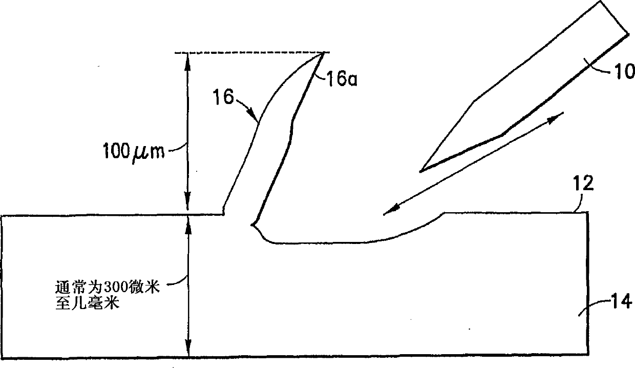
[0032] For example, in this application's Figure 2-6 A substrate with a Si device or chip mounted thereon in accordance with an embodiment of the present invention is shown in . In a preferred embodiment, as image 3 As shown, needle tool 10 is used to gouge on top metal surface 12 of substrate 14 to form substantially vertical protrusions 16 (or swarfs) extending upwardly from surface 12 of substrate 14 . As shown, the protrusions 16 preferably have a height of about 100 μm. While this is the preferred height for the protrusions 16, the height of the protrusions can be modified to suit a particular application.

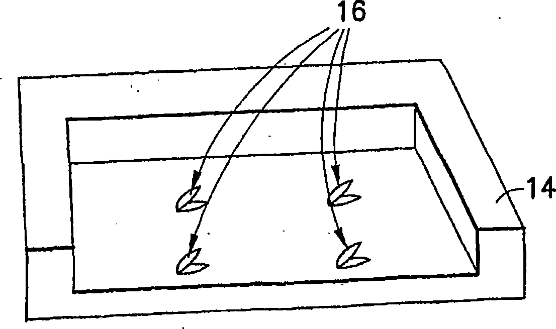
[0033] In a preferred embodiment, the substrate 12 is a metal can such as Metal cans used in product lines, or Cu layers such as the horseshoe-shaped DBC described above in the co-pending application entitled PACKAGE FOR HIGH POWER DENSITY DEVICES. However, protrusions 16 can equally be formed on any substrate, if desired. In a preferred embodiment, as figure...


PUM


Abstract

A substrate on which a silicon device is mounted in accordance with an embodiment of the present invention includes a plurality of protrusions extending upward from a top surface of the substrate and a solder layer formed on the top of the substrate such that the plurality of protrusions extends through the solder layer and a top portion of each protrusion of the plurality of protrusions is stamped down to be level with a top surface of the solder layer such that the silicon device is supported on the plurality of protrusions when placed on the substrate. The protrusions are preferably gouged up from the surface of the substrate with a needle like tool. A stamper tool is used to stamp the protrusions down to their desired height such that they are properly positioned to support the silicon device. The solder layer may be a solder pre-form or may be a layer of solder paste.

Description

[0001] Cross References to Related Applications [0002] This application claims the benefit of and priority to US Provisional Patent Application No. 60 / 756,738, filed January 6, 2005, entitled SOLDER THICKNESSCONTROL FOR BOND WIRELESS DISCRETE Si PACKAGE, which is hereby incorporated by reference in its entirety. Background technique [0003] Advances in semiconductor technology have pushed the performance limits of silicon beyond the capabilities of current packaging. In particular, the power and current carrying capabilities of MOSFETS and IGBTs are often limited by insufficient packaging capabilities. The thermal and electrical resistance of the package causes power loss and corresponding heating of the silicon beyond its limits. In addition, the inductance of the package causes some limitations in the use of high switching currents. In particular, parasitic package inductance can cause inductive overvoltages that can destroy silicon devices (Si devices). This is especi...

Claims


Application Information

Patent Timeline
Patent Type & Authority Applications(China)
IPC IPC(8): H01L23/48
CPCH01L2224/73153H01L2924/15153H01L2924/0105H01L21/4853H01L2924/01082H01L2224/83101H01L23/49811H01L24/32H01L24/39H01L2924/13091H01L2924/01327H01L2224/83801H01L2924/01029H01L2224/29111H01L2924/0132H01L2224/83192H01L2924/01027H01L2224/83136H01L2924/014H01L2924/30107H01L2924/01003H01L2924/18301H01L2224/32057H01L2924/0001H01L24/33H01L2924/01047H01L2924/0133H01L2924/01079H01L2224/83385H01L24/83H01L24/29H01L2924/01033H01L2924/01006H01L2924/15165H01L2224/8314H01L2924/10253H01L2924/01077H01L2924/13055H01L2924/1305H01L2224/32503H01L2224/8381H01L2924/15747H01L2924/00H01L2924/00015H01L2224/29099H01L23/52
Inventor H·豪恩施泰因
Owner INTERNATIONAL RECTIFIER COEP
Features
  • R&D
  • Intellectual Property
  • Life Sciences
  • Materials
  • Tech Scout
  • Unparalleled Data Quality
  • Higher Quality Content
  • 60% Fewer Hallucinations
Learn More