Enhancement of remote plasma source clean for dielectric films

A remote plasma and cleaning technology, applied in the field of strengthening the cleaning of remote plasma sources for dielectric films, can solve problems such as unpleasant negative effects

Inactive Publication Date: 2009-03-04
APPLIED MATERIALS INC
View PDF3 Cites 132 Cited by
  • Summary
  • Abstract
  • Description
  • Claims
  • Application Information

AI Technical Summary

Problems solved by technology

It has been found that the methods used to remove material from other dielectric layers, such as carbon-free silicon oxide layers, have had undesirable side effects and are not always sufficient to remove material from low-dielectric layers. Deposition of a constant film layer (which has a high carbon content) removes carbon

Method used


Image

  • Enhancement of remote plasma source clean for dielectric films
  • Enhancement of remote plasma source clean for dielectric films
  • Enhancement of remote plasma source clean for dielectric films

Examples


example 1

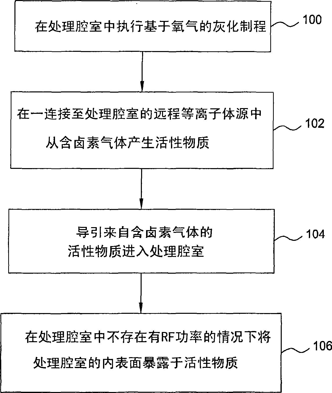
[0065] The chamber is cleaned by the following procedure: Generating reactive oxygen species and reactive fluorine species in a remote plasma source; directing reactive oxygen species and reactive fluorine species into chamber; and in the absence of RF power in the chamber the inner surface of the chamber was exposed to the active material for 150 seconds to remove about 6000 Angstroms of the low dielectric constant film containing silicon, oxygen and carbon. The low-k film layer has been previously deposited in the chamber in a PECVD process from a mixture containing methyldiethoxysilane (mDEOS), norbornadiene (BCHD), and oxygen. Reactive oxygen species were introduced into the chamber from a remote plasma source at a flow rate of approximately 6000 seem. Reactive fluorine species were introduced into the chamber from a remote plasma source at a flow rate of approximately 500 sccm. Helium was used as a carrier gas and flowed into the chamber at a flow rate of about 6000...


PUM


Abstract

Methods for cleaning semiconductor processing chambers used to process carbon-containing films, such as amorphous carbon films, barrier films comprising silicon and carbon, and low dielectric constant films including silicon, oxygen, and carbon are provided. The methods include using a remote plasma source to generate reactive species that clean interior surfaces of a processing chamber in the absence of RF power in the chamber. The reactive species are generated from an oxygen-containing gas, such as O2, and / or a halogen-containing gas, such as NF3. An oxygen-based ashing process may also be used to remove carbon deposits from the interior surfaces of the chamber before the chamber is exposed to the reactive species from the remote plasma source.

Description

technical field [0001] Embodiments of the invention generally relate to methods of cleaning processing chambers using a remote plasma source. Background technique [0002] The size of integrated circuit geometries has decreased dramatically since such devices were first introduced decades ago. Since then, integrated circuits have generally followed the two-year / half-size rule (commonly known as Moore's Law), which means that the number of devices on a chip doubles every two years. Today's fabrication facilities are routinely fabricating devices with 0.13 micron and even 0.1 micron feature sizes, and tomorrow's facilities will be fabricating devices with even smaller feature sizes. [0003] One that has contributed to the development of such small device sizes has been the development of patterned films that can be finely patterned and have the ability to transfer fine patterns through the underlying layers of the substrate. An example of such a patterned film is an amorpho...

Claims


Application Information

Patent Timeline
Patent Type & Authority Applications(China)
IPC IPC(8): B08B6/00B08B9/00
Inventor T·诺瓦克K·S·伊姆S-Y·B·唐K·D·李V·N·T·恩古耶D·辛格尔顿M·J·西蒙斯K·杰纳基拉曼G·巴拉苏布拉马尼恩M·阿优伯W·H·叶A·T·迪莫斯H·M'沙迪
Owner APPLIED MATERIALS INC
Why Eureka
Try Eureka