Supercharge Your Innovation With Domain-Expert AI Agents!

Electronic component

A technology of electronic components and terminals, which can be applied to computer parts, record carriers used by machines, instruments, etc., and can solve problems such as insufficient joint strength and insufficient reliability

Active Publication Date: 2009-03-11
HALLYS CORP
View PDF1 Cites 0 Cited by
  • Summary
  • Abstract
  • Description
  • Claims
  • Application Information

AI Technical Summary

Problems solved by technology

That is, if the bonding strength between the interposer and the base circuit board is insufficient, there may be a possibility that the reliability cannot be sufficiently ensured

Method used


Image

  • Electronic component
  • Electronic component
  • Electronic component

Examples


Embodiment 1

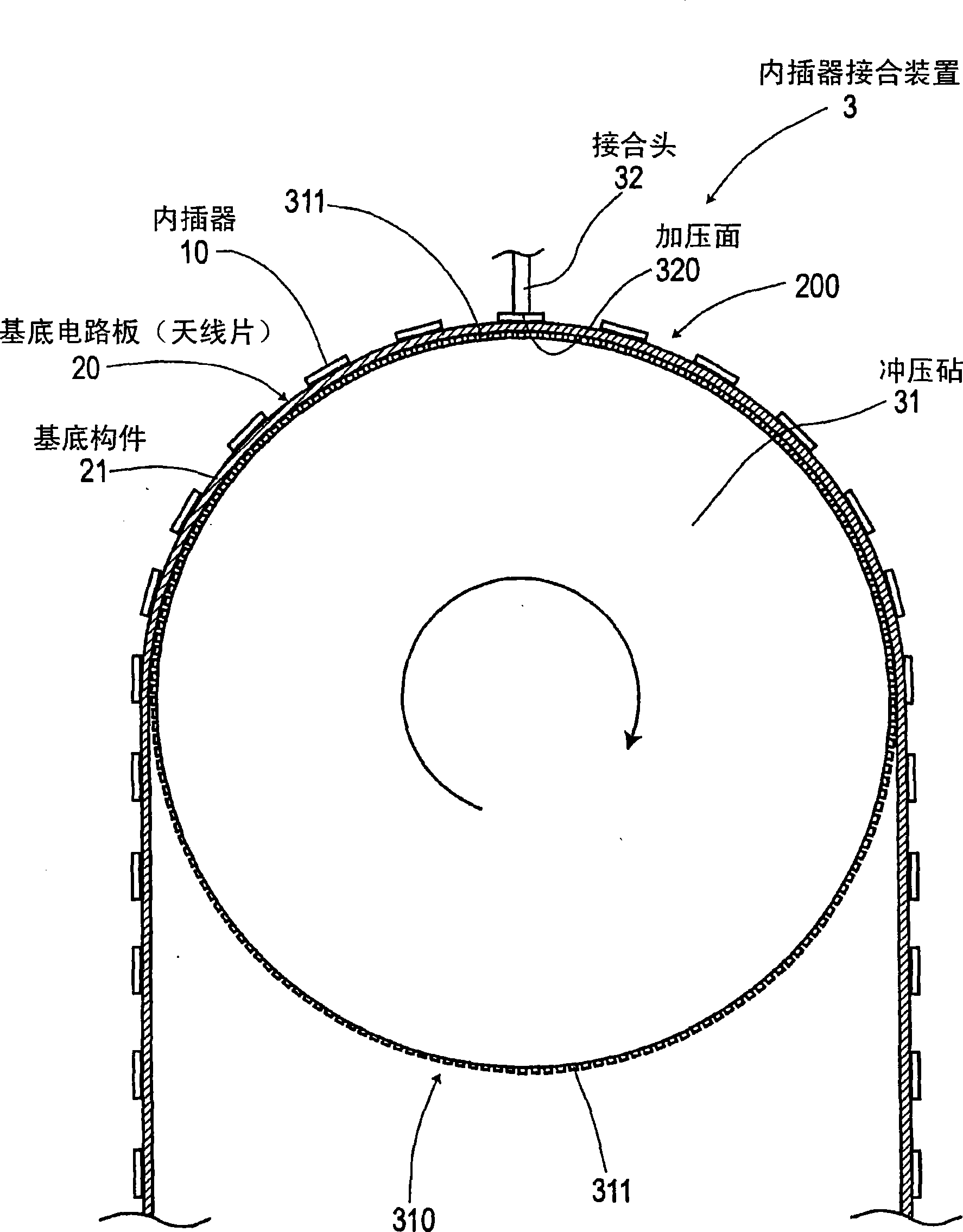
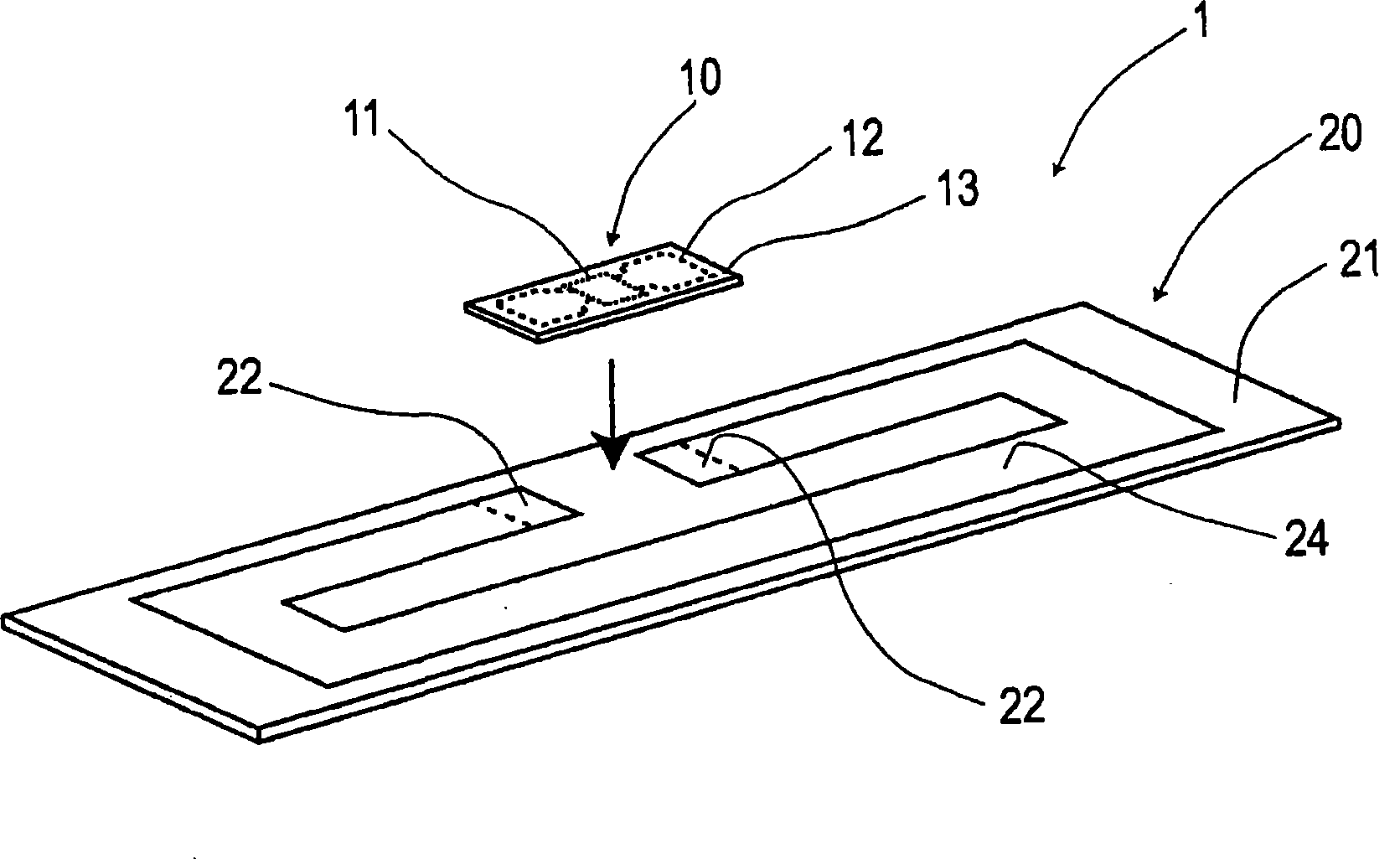
[0065] This example relates to an electronic component 1 in which an interposer 10 and a base circuit board 20 are bonded, and an interposer bonding apparatus 3 for manufacturing the electronic component 1 . refer to Figure 1 to Figure 9 Describe the content.

[0066] The interposer joint device 3 of this example is as figure 1 with figure 2 Shown is an interposer 10 configured for mounting a semiconductor chip 11 on a plate-shaped chip holding member 13 and having an interposer-side terminal 12 as a connection terminal extending from the semiconductor chip 11. A device that is bonded to a base circuit board 20 composed of a plate-shaped base member 21 and provided with base-side terminals 22 on its surface.

[0067] This interposer bonding device 3 has: a stamping anvil 31 that holds the base circuit board 20 on which the interposer 10 is stacked in a state where the interposer-side terminal 12 and the base-side terminal 22 face each other; The stamping anvil 31 perform...

Embodiment 2

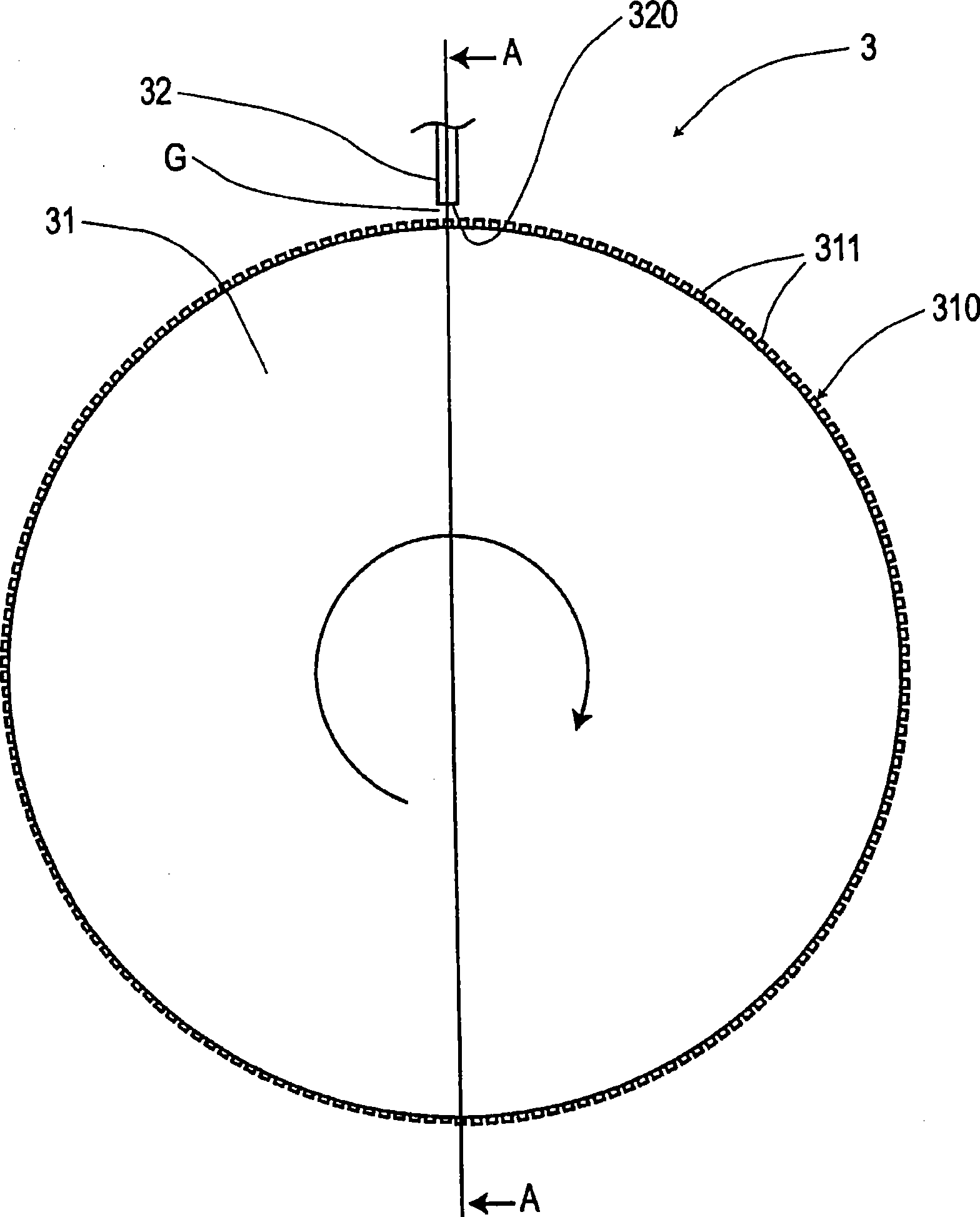
[0101] This example is based on the interposer joining device 3 of the first example, and mainly changes the shapes of the pressing surface 320 of the joining head 32 and the convex forming portion 310 of the press anvil 31 . refer to Figure 11 to Figure 16 Describe the content.

[0102] In the interposer joint device 3 of this example, as Figure 11 As shown, the bonding head 32 is in contact with the antenna board 20 , and the stamping anvil 31 is in contact with the interposer 10 .

[0103] The bonding head 32 of this example is as Figure 11 and Figure 12 As shown, there is a pressing surface 320 formed in a curved concave shape corresponding to the curved outer peripheral surface of the press anvil 31 . The pressing surface 320 is wider than the interposer 10 in the circumferential direction of the press anvil 31 . Therefore, in the interposer joining device 3 of this example, the entire surface of the interposer-side terminal 12 can be simultaneously pressurized by ...


PUM


Abstract

An electronic device (1) bonds an interposer (10) having an interposer-side terminal (12) to a base circuit sheet (20) provided with a base-side terminal. The base circuit board (20) is equipped with a plurality of base-side terminals (22) forming a plurality of protruded deformation portions (220) on the surface of the base member (21). The front portion of the protruded deformation portion (220) contacts with the interposer-side terminal (12) to ensure electric conduction. Moreover, a binder configuration layer (25) for an insulating binder with electrical insulating property is formed between the interposer-side terminal (12) and the base-side terminal (22).

Description

[0001] This application is a divisional application with a filing date of December 3, 2005, an application number of 200580041649.7, and an invention name of "Interposer Engaging Device". technical field [0002] The present invention relates to an electronic component obtained by bonding an interposer having interposer-side terminals to a base circuit sheet. Background technique [0003] Conventionally, there is an RF-ID medium in which, for example, an interposer in which an IC chip is mounted on a resin film is laminated and bonded to an antenna board as a base circuit board. When producing such electronic components such as RF-ID media, for example, an interposer and an antenna board laminated with an adhesive are sometimes pressed along the lamination direction. In this way, as an interposer bonding device for press-bonding an interposer and an antenna board, for example, the interposer and the antenna board are disposed in a gap between a pair of stamping dies facing e...

Claims


Application Information

Patent Timeline
Patent Type & Authority Applications(China)
IPC IPC(8): G06K19/077
Inventor 西川良一青山博司
Owner HALLYS CORP
Features
  • R&D
  • Intellectual Property
  • Life Sciences
  • Materials
  • Tech Scout
  • Unparalleled Data Quality
  • Higher Quality Content
  • 60% Fewer Hallucinations
Learn More