Image sensor and method for manufacturing same
An image sensor and junction technology, applied in semiconductor/solid-state device manufacturing, electrical solid-state devices, semiconductor devices, etc., can solve problems such as free movement of photocharges, generation of dark current, reduction of saturation and sensitivity, etc.
- Summary
- Abstract
- Description
- Claims
- Application Information
AI Technical Summary
Problems solved by technology
Method used
Image

Examples
Embodiment Construction
[0017] Hereinafter, embodiments of the image sensor will be described in detail with reference to the accompanying drawings.
[0018] In the description of the embodiments, when it is mentioned that a layer (or film) is "on" another layer or substrate, it can be understood that the layer (or film) is directly on another layer or substrate, or where Intermediate layers can occur. Further, when it is mentioned that a layer is "under" another layer, it can be understood that the layer may be directly under the other layer, or one or more intervening layers may be interposed therebetween. In addition, when a layer is referred to as being "between" two layers, it can also be understood that only that layer is between the two layers, or one or more intervening layers may also be present.
[0019] The present disclosure is not limited to complementary metal-oxide-semiconductor (CMOS) image sensors, but can be applied to any image sensor that requires a photodiode.
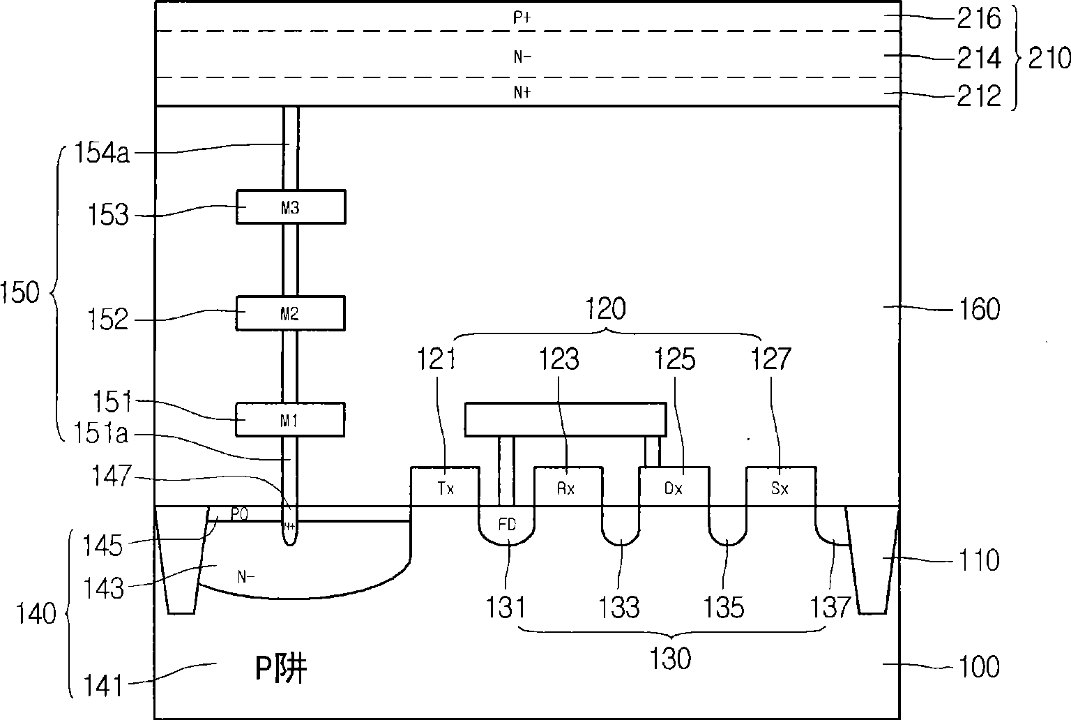
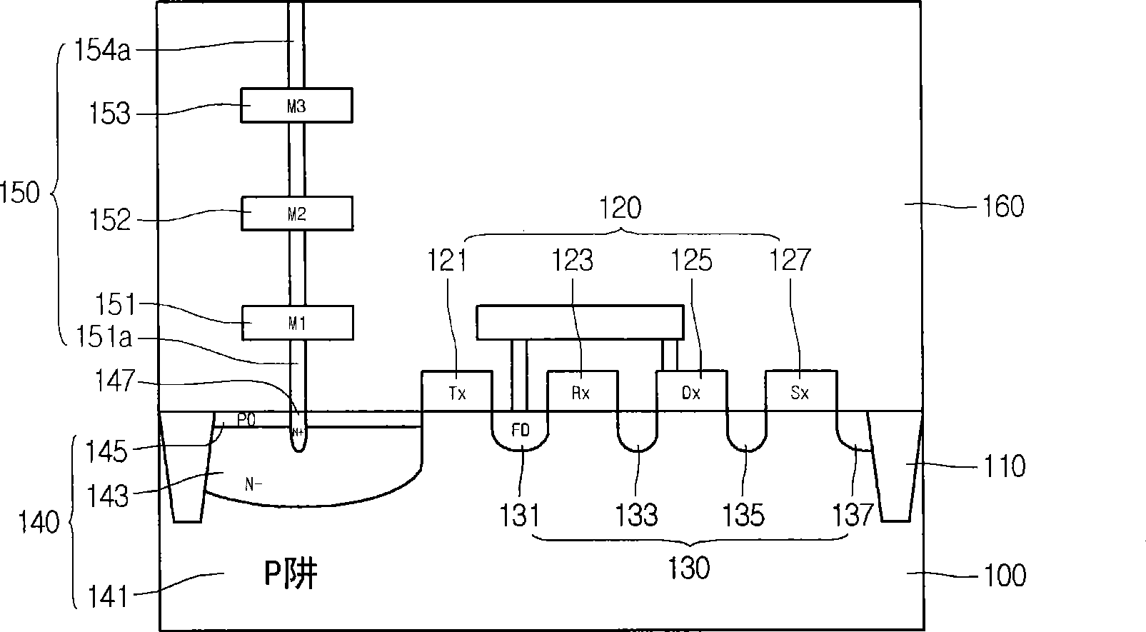
[0020] figure ...
PUM
 Abstract
Description
Claims
Application Information