Member for plasma display and method for producing the same
A display and component technology, applied in the direction of AC plasma display panels, electrical components, solid cathode components, etc., can solve the problems of lowering the height of the main barrier, deteriorating the display characteristics of the PDP panel, and not being able to fully utilize the main barrier separating the electric space , to achieve the effect of solving false light emission
- Summary
- Abstract
- Description
- Claims
- Application Information
AI Technical Summary
Problems solved by technology
Method used
Image

Examples
Embodiment 1
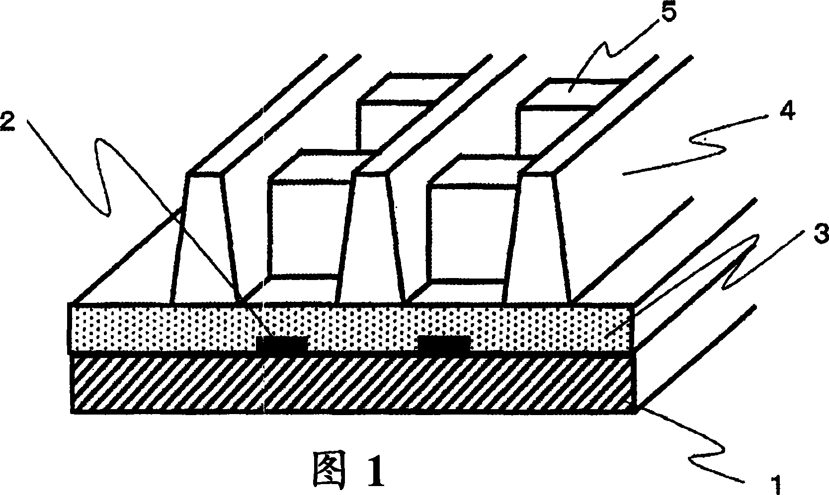
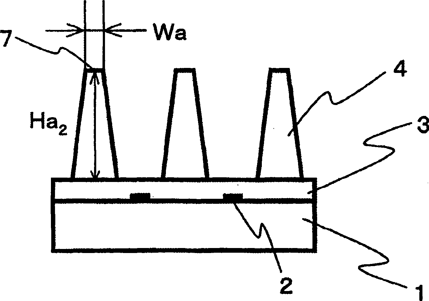
[0214] Address electrodes were fabricated on a glass substrate PD200 (size: 964×570 mm) with photosensitive silver paste. The photosensitive silver paste was coated, dried, exposed, developed and fired to form address electrodes with a line width of 20 μm, a thickness of 3 μm, and a pitch of 100 μm.
[0215] 0080
[0216] Next, 60% by weight of low-melting glass powder containing 75% by weight of bismuth oxide, 10% by weight of titanium oxide powder with an average particle size of 0.3 μm, 15% by weight of ethyl cellulose, and 15% by weight of terpineol were mixed to obtain glass paste. Then, screen printing is used to coat the glass paste with a thickness of 20 μm to cover the bus bar electrodes of the display part, and then bake at 570° C. for 15 minutes to form a dielectric layer.
[0217] 0081
[0218] Coat the photosensitive paste on the dielectric layer. The photosensitive paste is composed of glass powder and organic components containing photosensitive components. ...
Embodiment 2~5、 comparative example 1~3
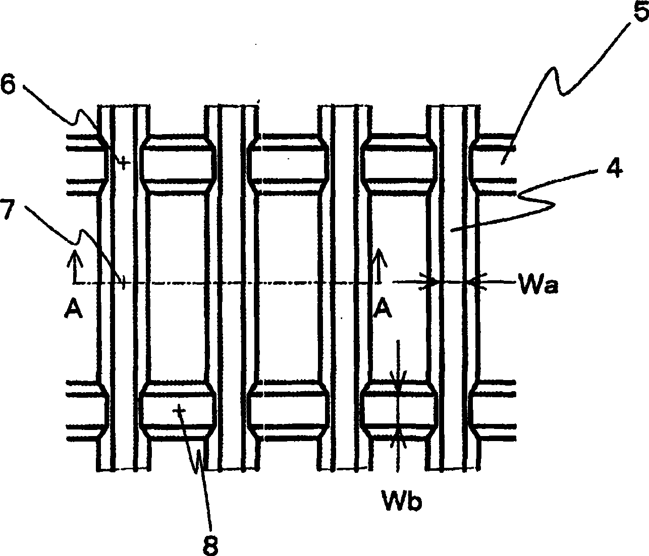
[0227] Adopting and implementing In the same manner as in Example 1, a member for a plasma display was obtained. Table 1 shows properties of the obtained member for a plasma display. In Example 2, Wb / Wa was 2.5, and the height difference of the main barrier rib was slightly large at 5 μm, but there was no problem in use. The Wb / Wa of Examples 3 and 4 are 1.3, the Wb / Wa of Example 5 is 1.5, and the Wb / Wa of Example 6 is 1.4. The height differences of the respective main barrier ribs are 1 μm, 4 μm, 5 μm, and 2 μm, respectively. In Examples 4 and 5, since Ha2-Hb is large, the height difference of the main barrier ribs is slightly larger, but there is no problem in use. In the members for plasma displays of Comparative Examples 1, 2, and 3, Wb / Wa was less than 1.2, and there was a problem that the height of the main barrier rib in the partition portion was low.
[0228] 0086
[0229] Table 1
[0230]
PUM
| Property | Measurement | Unit |
|---|---|---|
| thickness | aaaaa | aaaaa |
| particle diameter | aaaaa | aaaaa |
| particle diameter | aaaaa | aaaaa |
Abstract
Description
Claims
Application Information