Display device with flip-chip structure

A display device and flip-chip technology, which is applied to electrical components, electrical solid devices, circuits, etc., can solve problems such as uneven distribution of connection bumps, uneven pressure, and poor bonding of conductive particles

Inactive Publication Date: 2009-04-22
INNOLUX CORP +1
View PDF0 Cites 4 Cited by
  • Summary
  • Abstract
  • Description
  • Claims
  • Application Information

AI Technical Summary

Problems solved by technology

[0004] However, the design of the connection bumps on the general integrated circuit chip often only considers the functionality, while ignoring the uniform symmetry of the structure, so the positions of the connection bumps on the integrated circuit chip are mostly unevenly distributed.
In the case of uneven distribution of connection bumps, uneven pressure will occur during the bonding process, cau

Method used


Image

  • Display device with flip-chip structure
  • Display device with flip-chip structure
  • Display device with flip-chip structure

Examples


Embodiment Construction

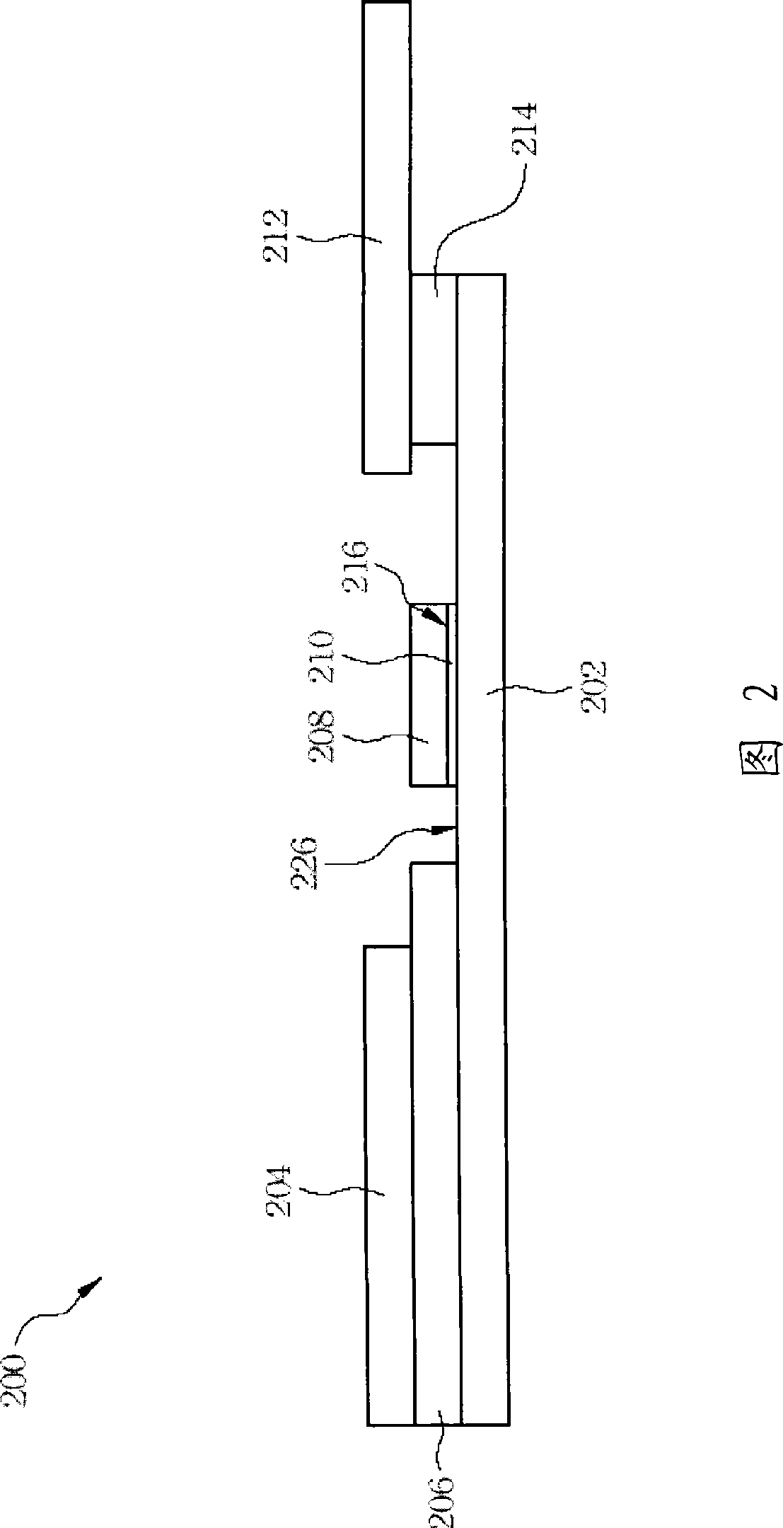
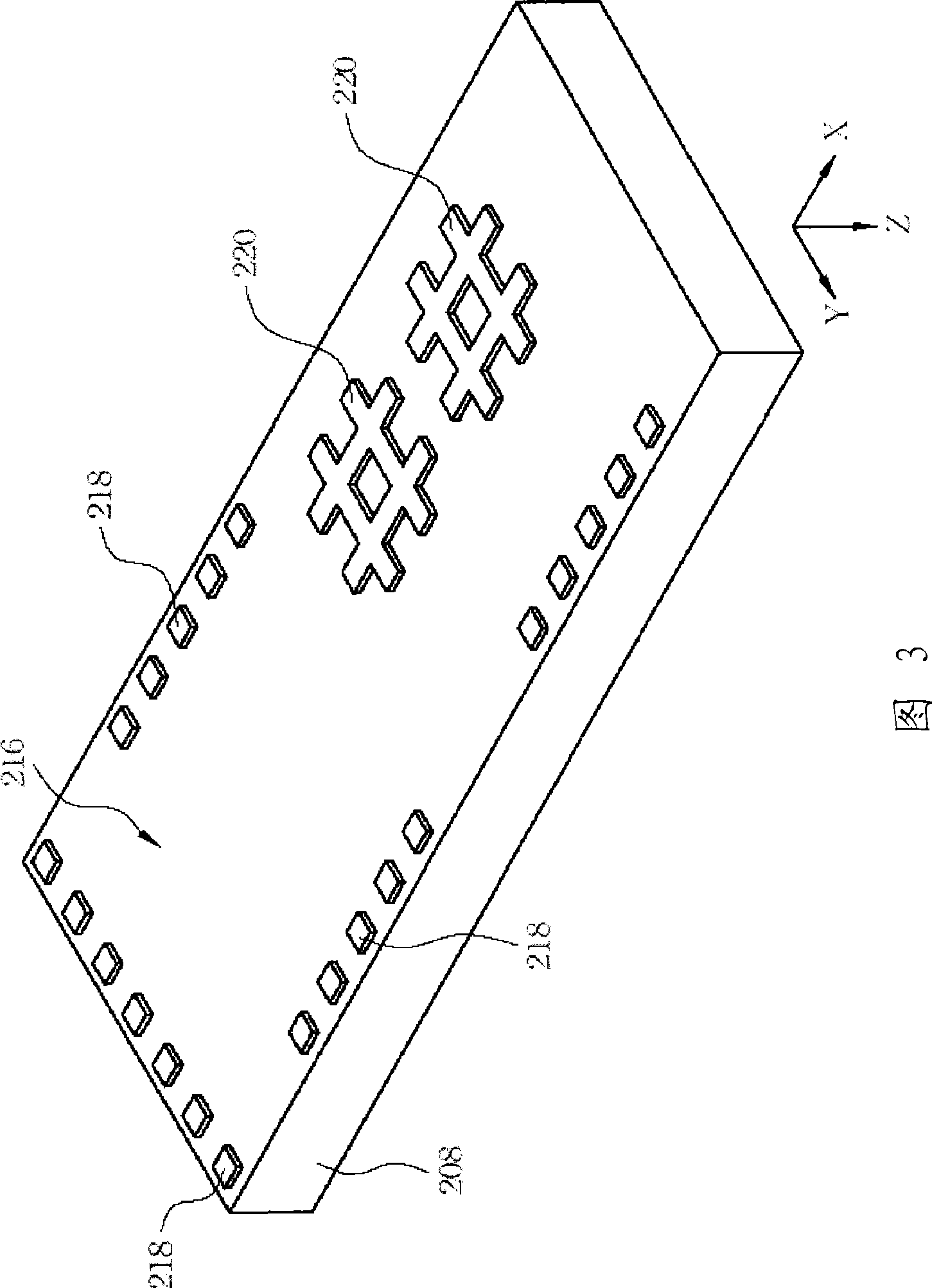
[0028] The invention discloses a display device with a flip-chip structure, which can greatly improve the lamination yield of the flip-chip process, and can strengthen the structural strength of the integrated circuit chip. In order to make the description of the present invention more detailed and complete, reference may be made to the following description together with the illustrations in FIGS. 2 to 4B .

[0029] Please refer to FIG. 2 , which is a schematic cross-sectional view of part of a display device with a flip-chip structure according to a preferred embodiment of the present invention. The display device 200 with a flip-chip structure includes a first substrate 202, wherein a display layer 206 is disposed on the first substrate 202, and the material of the first substrate 202 can be glass or a flexible substrate. In this exemplary embodiment, the display device 200 may further include a second substrate 204 covering the first substrate 202, wherein the material of ...


PUM


Abstract

The invention discloses a display device with a flip-chip structure, the display device at least comprises a first substrate and at least one integrated circuit chip which is arranged on the first substrate, wherein, a plurality of connecting bumps are arranged on one surface of the integrated circuit chip, the connecting bumps are connected between the integrated circuit chip and the first substrate; and the display device also comprises at least one Dummy Bump which is clamped between the integrated circuit chip and the first substrate for balancing the distribution of the connecting bumps on the surface of the integrated circuit chip.

Description

technical field [0001] The present invention relates to a display device, and in particular to a display device with a flip chip structure (Flip Chip). Background technique [0002] In a display device with a flip-chip structure, a plurality of welding bumps (Bumps) are provided on the lower surface of an integrated circuit (IC) chip for electrical bonding between the IC chip and a display panel of the display device. [0003] Please refer to FIG. 1 , which is a schematic partial cross-sectional view of a conventional display device with a flip-chip structure. When bonding the integrated circuit (IC) chip 108 on the display panel 102 of the display device 100, usually a layer of anisotropic conductive film (Anisotropic Conductive Film) 104 is first coated on the display panel 102, and then the integrated circuit chip 108 is placed and pressed. on the anisotropic conductive adhesive 104, so that the integrated circuit chip 108 is glued on the display panel 102 by using the a...

Claims


Application Information

Patent Timeline
IPC IPC(8): H01L23/00H01L23/485H01L23/488
Inventor 陈圣伟林志展
Owner INNOLUX CORP
Why Eureka
Try Eureka