A method for realizing nor FLASH bad block management and its control circuit
A technology for controlling circuits and bad blocks, applied in the field of FLASH flash memory, can solve the problems of taking up system execution time, cumbersome management and update backup, etc., and achieve the effect of high erasing and writing endurance
- Summary
- Abstract
- Description
- Claims
- Application Information
AI Technical Summary
Problems solved by technology
Method used
Image

Examples
Embodiment Construction
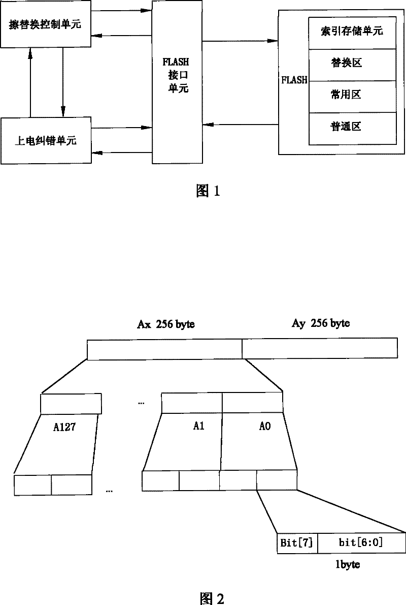
[0026] see figure 1 , the present invention includes FLASH divided into common area, frequently used area and replacement area. The common area and frequently used area are accessible areas of the system bus, and the common area cannot be replaced. The common area can replace the logical address of the bad block through the replacement area, and the replacement area is the replacement backup area of the common area. The invention also includes an erasing and replacing control unit for controlling FLASH erasing and replacing, a power-on error correction unit for checking and verifying write errors when the system is powered on, an index storage unit, and a FLASH interface unit for controlling FLASH erasing and writing timing. The erase replacement control unit and the power-on error correction unit are connected to each other and respectively to the FLASH interface unit, and the FLASH interface unit is connected to the index storage unit and the FLASH. The erasing and repla...
PUM
 Abstract
Description
Claims
Application Information
 - R&D
- Intellectual Property
- Life Sciences
- Materials
- Tech Scout
- Unparalleled Data Quality
- Higher Quality Content
- 60% Fewer Hallucinations
Browse by: Latest US Patents, China's latest patents, Technical Efficacy Thesaurus, Application Domain, Technology Topic, Popular Technical Reports.
© 2025 PatSnap. All rights reserved.Legal|Privacy policy|Modern Slavery Act Transparency Statement|Sitemap|About US| Contact US: help@patsnap.com