Gate drive circuit and drive method thereof

A gate drive circuit and circuit technology, applied in the direction of logic circuit, logic circuit connection/interface layout, logic circuit coupling/interface using field effect transistors, etc., can solve the problems of increasing components and increasing costs, so as to reduce consumption, Reduce the effect of using

Active Publication Date: 2010-11-03
HOLTEK SEMICON
View PDF4 Cites 0 Cited by
  • Summary
  • Abstract
  • Description
  • Claims
  • Application Information

AI Technical Summary

Problems solved by technology

But in this way, it will increase the number of components and further increase the cost

Method used


Image

  • Gate drive circuit and drive method thereof
  • Gate drive circuit and drive method thereof
  • Gate drive circuit and drive method thereof

Examples


Embodiment Construction

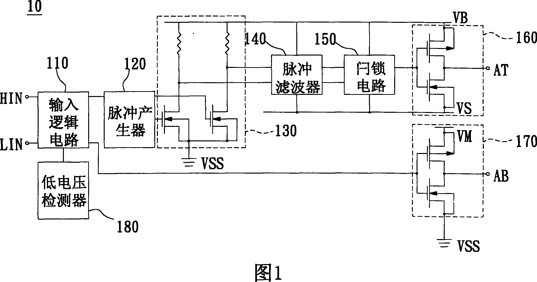
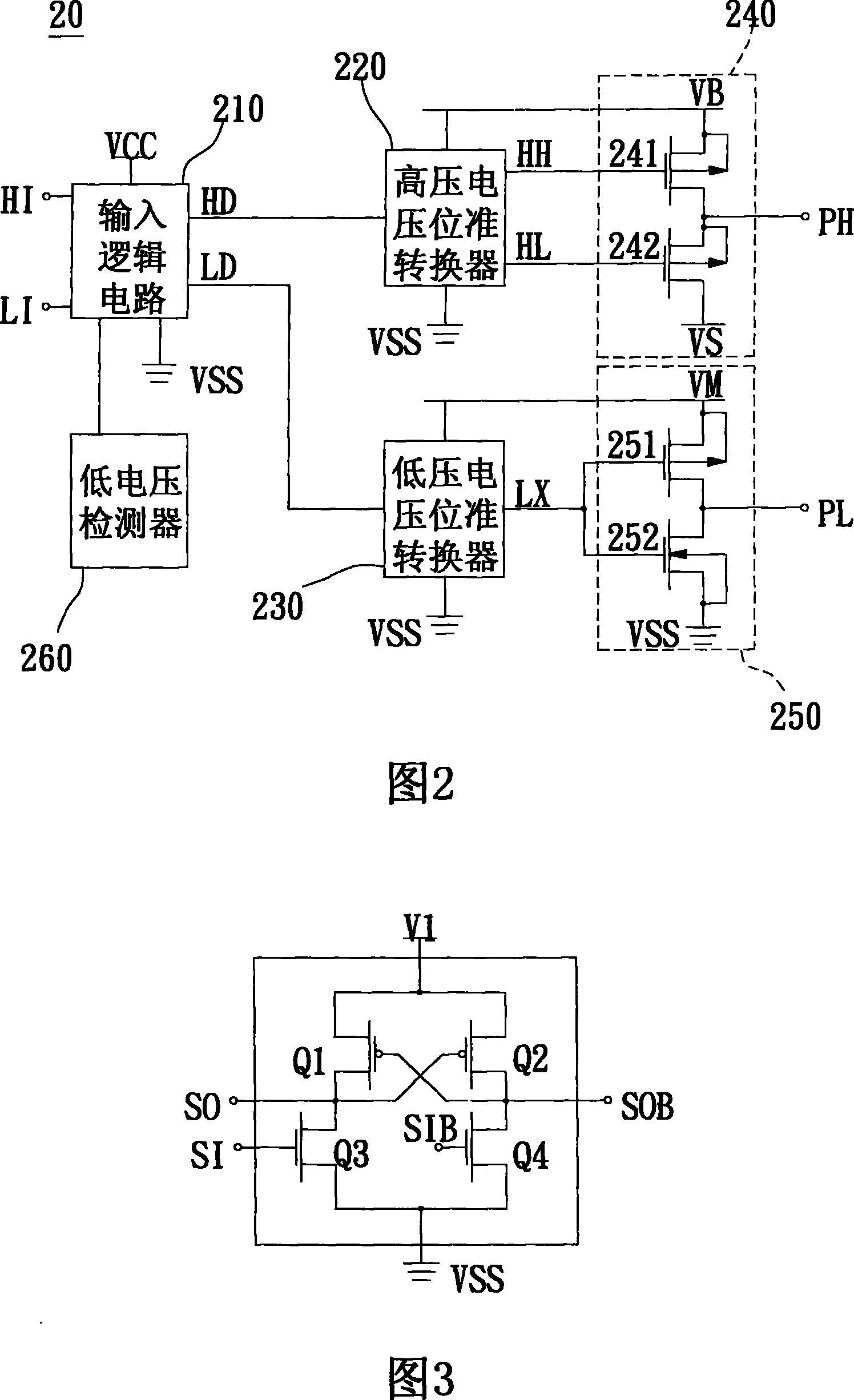
[0043] Please refer to figure 2 , which is a schematic block diagram of the gate driving circuit of the present invention. The gate driving circuit 20 of the present invention includes an input logic circuit (input logic circuit) 210, a high voltage voltage level shifter (high voltage level shifter) 220, a low voltage voltage level shifter (low voltage level shifter) 230, A high side driver 240 , a low side driver 250 and a low voltage detector 260 .

[0044] The input logic circuit 210 receives an input signal through the signal input terminals HI and LI, and converts the input signal into a high side signal (highside signal) HD and a low voltage side signal (low side signal) through the operation of the internal circuit of the input logic circuit 210 side signal) LD. Wherein, the voltage operation range of the input logic circuit 210 is between VSS and VCC. VSS and VCC can be designed to be 0V and 5V respectively, but they can also be different due to different actual ap...


PUM


Abstract

The invention discloses a gate drive circuit and a drive method thereof. A voltage-level converter converts the voltage operation level range of an input end signal so as to reduce use of circuit components and lower cost; and a driver stage output component on the high voltage end adopts a P type metal-oxide semiconductor field effect transistor, which is connected in series, to be used as a diverter switch, thereby preventing the matrix effect generating in the general process of manufacturing at a high voltage.

Description

technical field [0001] The present invention relates to a driver, in particular to a gate driving circuit and a driving method thereof. Background technique [0002] Because some specific application circuits require a component with a huge driving capability, the component is usually a power transistor, and in order to control the power transistor to drive these application circuits, a control signal must be input to the gate terminal of the power transistor. Therefore, the power transistor will A gate drive circuit is configured in the preceding stage. For example, the driving principle of a motor is to control the high-voltage side power transistor and the low-voltage side power transistor according to a specific connection method to turn on and off in order to make the motor rotate. In order to turn on or off the power transistor, a high-state or low-state control signal must be input at its gate terminal, but due to the control signal input at the gate terminal of the ...

Claims


Application Information

Patent Timeline
Patent Type & Authority Patents(China)
IPC IPC(8): H03K17/687H03K19/0185H03K19/0944
Inventor 陈俊雄张逸泰刘温良
Owner HOLTEK SEMICON
Why Eureka
Try Eureka