
Socket contact terminal and semiconductor device

A technology for sockets and terminals, which is applied in the field of contact terminals for sockets, can solve the problems of inability to remove the oxide film of the connection pad, heat generation or increased voltage drop, and high contact resistance, and achieve the effect of good processing ease

Inactive Publication Date: 2011-12-21
THE FUJIKURA CABLE WORKS LTD
View PDF8 Cites 0 Cited by
  • Summary
  • Abstract
  • Description
  • Claims
  • Application Information

AI Technical Summary

Problems solved by technology

[0014] However, if the conductive elastic member disclosed in Patent Document 3 is used, since the contact terminal is not a metal but an elastic member, the contact resistance is high compared with a metal contact, and there is a problem of heat generation or Possibility of voltage drop increases. When inserting into the package, since the contact terminal does not rub against the metal land, new problems such as the inability to remove the oxide film on the land will arise.

Method used


Image

  • Socket contact terminal and semiconductor device
  • Socket contact terminal and semiconductor device
  • Socket contact terminal and semiconductor device

Examples


no. 1 Embodiment approach

[0175] Hereinafter, embodiments of the present invention will be described with reference to the accompanying drawings.

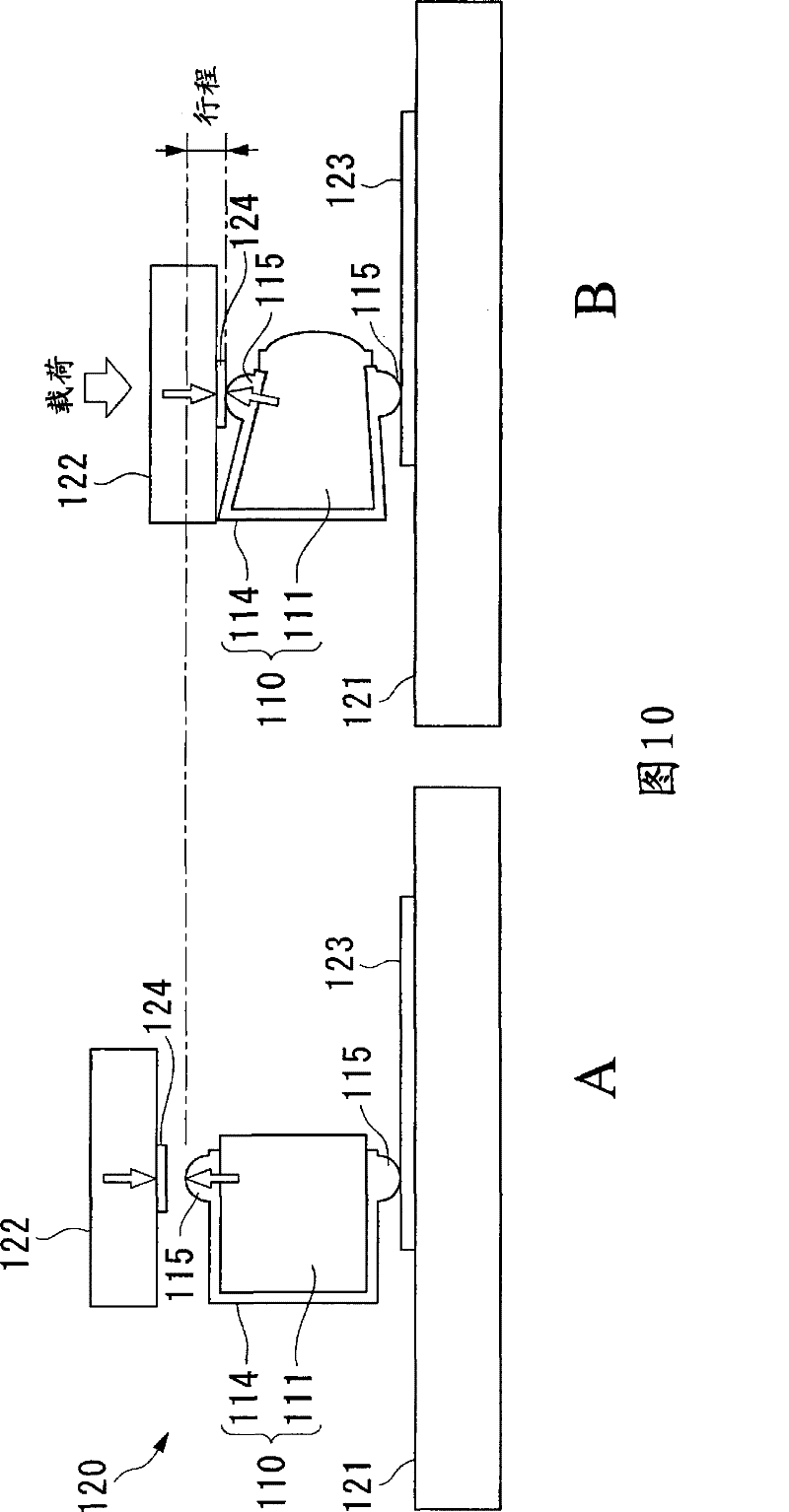
[0176] Figures 1A-1D It is a figure which shows the 1st Embodiment of the contact terminal for sockets of this invention (Hereinafter, it is abbreviated as contact terminal.), Figure 1A is a side view of the contact terminal 10, Figure 1B is a top view, Figure 1C is the main view, Figure 1D is the rear view. In these figures, reference numeral 10 is a contact terminal, 11 is a metal terminal, 12 is an elastic member, 13 is a main column portion, 14 is an arm portion, and 15 is a contact portion.

[0177] The contact terminal 10 of the present embodiment provides electrical conduction between the connection portion made of a metal conductor on the printed circuit board and the connection terminal of the IC package, and includes a square U-shaped metal terminal 11 having a main column portion 13 and The arm parts 14 on both sides; and the rectangular...

no. 2 Embodiment approach

[0191] Figures 3A-3C It is a figure which shows 2nd Embodiment of the contact terminal of this invention. In FIG. 3, only the metal terminal 31 of the contact terminal 30 of this embodiment is shown. Figure 3A is a top view of the metal terminal 31, Figure 3B is a side view, Figure 3C is the rear view. In these figures, reference numeral 31 is a metal terminal, 32 is a main column portion, 33 is an arm portion, 34 is a wide and thick plate portion, and 35 is a dome-shaped convex portion.

[0192] The contact terminal 30 of the present embodiment is characterized in that it has substantially the same constituent elements as the contact terminal 10 of the first embodiment described above, and furthermore, a dome-shaped protrusion is provided on the outer surface of the arm portion 33 of the metal terminal 31 . At the same time, in the central part of the main column part 32, a wide thick plate part 34 having a wider width than other parts and a thicker plate than the oth...

no. 3 Embodiment approach

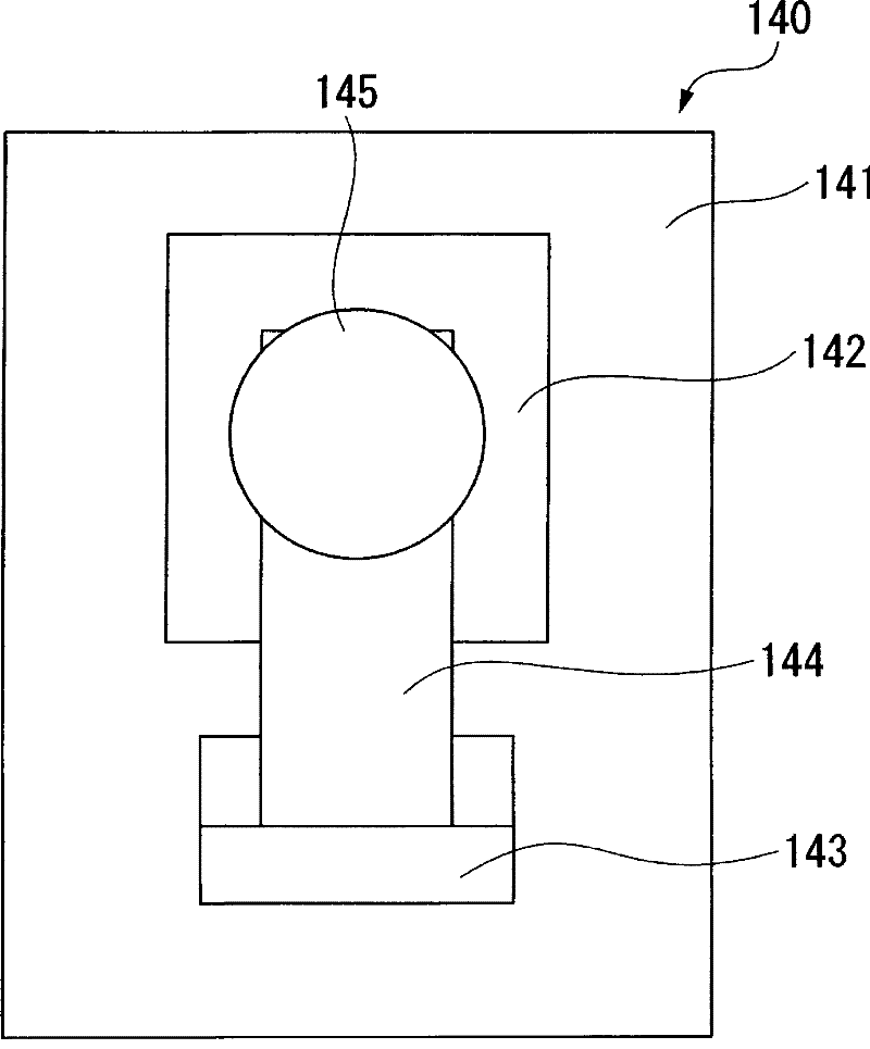
[0202] 4 is a view showing a third embodiment of the contact terminal of the present invention. In FIG. 4, only the metal terminal 41 among the contact terminals of this embodiment is shown. Figure 4A is a side view of the metal terminal 41, Figure 4B is a top view, Figure 4C is the rear view. In these figures, reference numeral 41 is a metal terminal, 42 is a main column portion, 43 is an arm portion, 44 is a wide and thick plate portion, and 45 is a semi-cylindrical convex portion.

[0203] The contact terminal of the present embodiment is characterized in that it has the same components as the contact terminal 30 of the second embodiment described above. In the present embodiment, the arm portion 43 of the metal terminal 41 is formed into a semi-cylindrical shape by bending. shaped convex portion 45 . In addition, like the contact terminal 30 of the second embodiment, the wide thick plate portion 44 is provided in the center of the main column portion 42, but the wid...


PUM


Abstract

A contact terminal for a socket, which is used to conduct conduction between a connection portion made of a metal conductor on a printed circuit board and a connection terminal of an IC package, and has a main column portion and two sides. A square U-shaped metal terminal on the arm, and an elastic member attached to the metal terminal. The metal surface is exposed on the outer surface of the arms of the metal terminal, and the elastic member is sandwiched between the arms so that when the arms are pressed in a direction approaching between the arms of the metal terminal, Play resilience.

Description

technical field [0001] The present invention relates to a contact terminal for an IC socket used when an IC package such as a CPU and an LSI is mounted on a printed circuit board, and particularly relates to an IC package suitable for mounting an LGA package and a BGA package on a printed circuit board. Contact terminals for sockets and semiconductor devices using them. [0002] This application claims based on Japanese Patent Application No. 2006-149510 filed with the Japan Patent Office on May 30, 2006, Japanese Patent Application No. 2006-154545 filed with the Japan Patent Office on June 2, 2006, and Japanese Patent Application No. 2006-154545 filed with the Japan Patent Office on June 7, 2006 Priority of Japanese Patent Application No. 2006-158670, Japanese Patent Application No. 2006-162508 filed with the Japan Patent Office on June 12, 2006, and Japanese Patent Application No. 2006-162509 filed with the Japan Patent Office on June 12, 2006, which are incorporated herein ...

Claims


Application Information

Patent Timeline
Patent Type & Authority Patents(China)
IPC IPC(8): H01R13/24H01R12/51H01R33/74H01R43/00
Inventor 大内康弘二阶堂伸一宫泽春夫渡边裕人山上胜哉
Owner THE FUJIKURA CABLE WORKS LTD
Learn More