Check patentability & draft patents in minutes with Patsnap Eureka AI!

Semiconductor miniature suspension structure and method of producing the same

A technology of suspension structure and manufacturing method, applied in semiconductor/solid-state device manufacturing, microstructure technology, microstructure device and other directions, can solve the problems of metal pollution in etching machine cavity, reduction of etching rate, pollution of micro-electromechanical structure, etc. The effect of reducing micro-loading effects, reducing high-precision requirements, and avoiding metal contamination

Inactive Publication Date: 2011-07-27
MEMSMART SEMICON
View PDF2 Cites 0 Cited by
  • Summary
  • Abstract
  • Description
  • Claims
  • Application Information

AI Technical Summary

Problems solved by technology

[0010] First, it adopts anisotropic dry chemical etching (anisotropic dry chemical etching) process to remove the insulating layer by means of chemical reaction. The substrate is etched a lot, so this technology will cause serious undercut;
[0011] Second, in the process of this commonly used technology, the MEMS structure is exposed to the process air after the initial etching. After a long multi-layer etching process, the MEMS structure is often polluted and damaged, causing The product yield rate is greatly reduced;
[0012] Third, the metal layer will be exposed to the outside during etching, which will cause the cavity of the etching machine to be polluted by metal, and cause the instability of the etching rate
[0013] The development of the above-mentioned technologies is very rapid. In order to improve many of its problems, the US patent 6712983B2 proposes the technology of using reactive ion etching (Reactive Ion Etching, hereinafter referred to as RIE). Although this technology can greatly reduce the undercut phenomenon (under cut) , but because it is also etched layer by layer from top to bottom, and the last large amount of etching work on the silicon substrate must be formed by using lateral etching technology, so this improved technology is still too cumbersome and complicated, and still through the microelectromechanical structure. A large amount of etching and lateral etching will still cause under cut
Importantly, the above-mentioned problems of MEMS structure exposure and affecting yield have not been improved
[0014] The problem that cannot be solved by various technologies today is that the commonly used technologies in the past still require a layer of precise photolithography mask to make the etching technology complete. However, the design of micro-electro-mechanical technology is becoming more and more sophisticated. , making the manufacture of photolithography masks more and more difficult, which not only increases the production cost, but also has various challenges of transmission, error, cost and pollution residues in precision photolithography masks made in different processes. These problems are still unsolvable in general technology, and are also the key points for continuous breakthroughs in the design, manufacturing and packaging of semiconductor microstructures
[0015] In addition, the smaller the pattern spacing of the photolithography mask, the smaller the etching opening area, the reactants or energetic ions in the etching system cannot reach the expected bottom, or the reaction products cannot be smoothly discharged out of the opening, making the etching The speed is reduced; the above-mentioned problems are more serious when the area is smaller, which is the so-called micro-loading effect (Micro loading Effect)

Method used


Image

  • Semiconductor miniature suspension structure and method of producing the same
  • Semiconductor miniature suspension structure and method of producing the same
  • Semiconductor miniature suspension structure and method of producing the same

Examples


Embodiment Construction

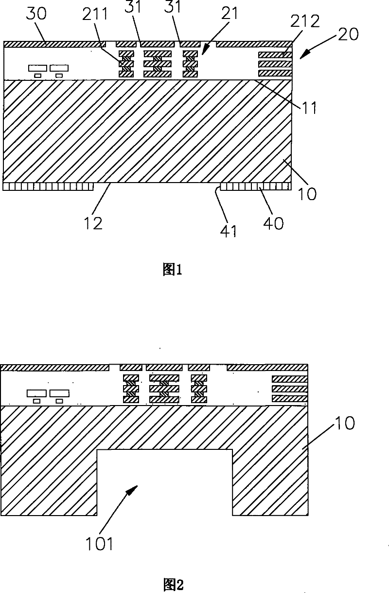
[0038] Figure 1 to Figure 7 As a specific embodiment of the present invention, the detailed description of the micro-suspension structure compatible with integrated circuits of the present invention and its manufacturing method is as follows:

[0039] (1) The structure of the present invention is as figure 1 As shown, first an insulating layer 20 with a microelectromechanical structure 21 is formed on the upper surface 11 of a silicon substrate 10. The microelectromechanical structure 21 includes at least one microstructure 211 and a plurality of metal circuits 212 that are independent of each other, and the microelectromechanical structure is in The surface of the insulating layer has an exposed portion 30, and the exposed portion 30 is provided with a through hole 31 corresponding to the expected etching space between the micro-electromechanical structure. The expected etching space only passes through the insulating layer 20 without contacting the micro-electro-mechanical ...


PUM


Abstract

The invention discloses a method for manufacturing a semiconductor micro-suspension structure, which is to form at least one insulating layer with a micro-electromechanical structure on the upper surface of a silicon substrate. The micro-electromechanical structure comprises at least one microstructure and one metal circuit which are independent with each other, and is provided with an exposed part on the surface of the insulating layer, wherein the exposed part is provided with a through hole or a metal bolt stacking layer corresponding to expectant etching space of the micro-electromechanical structure; the etching space or the metal bolt stacking layer only passes through the insulating layer; moreover, a mask layer of an opening is arranged on the surface of the insulating layer; the opening is arranged outside the through hole or the metal bolt stacking layer; and then space is formed by etching in sequence so as to make the micro-electromechanical structure suspended. Therefore,the method can effectively protect the micro-electromechanical structure from improper corrosion and exposure, can simplify photoetched mask plate technology, reduce high-precision requirement of the photoetched mask plate, and reduce cost. The invention also discloses a micro-suspension structure.

Description

technical field [0001] The invention relates to a semiconductor micro-suspension structure. The invention also relates to a preparation method of the semiconductor micro-suspension structure. Background technique [0002] Current semiconductor micro-electro-mechanical systems include various semiconductor microstructures, such as immovable probes, flow channels, and cavity structures, or some movable springs, connecting rods, and gears (rigid body motion or flexible deformation) and other structures. [0003] Various semiconductor applications can be formed by integrating the above-mentioned different structures and related semiconductor circuits; improving various functions of micro-mechanical structures through manufacturing methods is a key pointer for future semiconductor MEMS systems and a further step in the future. A serious challenge when researching chips. If the known technology can be developed and improved, the future development prospects cannot be predicted....

Claims


Application Information

Patent Timeline
Patent Type & Authority Patents(China)
IPC IPC(8): H01L21/00B81B3/00B81C1/00
Inventor 陈晓翔
Owner MEMSMART SEMICON
Features
  • R&D
  • Intellectual Property
  • Life Sciences
  • Materials
  • Tech Scout
  • Unparalleled Data Quality
  • Higher Quality Content
  • 60% Fewer Hallucinations
Learn More