Self-bias low-voltage operation transconductance amplifier circuit with controllable loop gain

A technology of transconductance amplifier and loop gain, which is applied in the direction of DC-coupled DC amplifier and differential amplifier, etc., which can solve the problems of difficult analog circuit design, harsh lithography precision, and circuit performance degradation, and achieve a gain/power consumption ratio Large, optimized performance, performance-enhancing effects

Active Publication Date: 2011-07-20
灿芯创智微电子技术(北京)有限公司
View PDF0 Cites 0 Cited by
  • Summary
  • Abstract
  • Description
  • Claims
  • Application Information

AI Technical Summary

Problems solved by technology

[0006] With the advancement of deep sub-micron technology, the channel size of the device is getting shorter and shorter, and the precision of lithography is becoming more and more demanding, and the resulting process fluctuations are also increasing.
This brings unimaginable difficulties to the design of analog circuits.
In order to ensure that the product reaches a certain yield rate and increase product profits, the design of the analog circuit must leave enough margin to meet the requirements of process fluctuations, but this will also lead to a decline in circuit performance

Method used


Image

  • Self-bias low-voltage operation transconductance amplifier circuit with controllable loop gain
  • Self-bias low-voltage operation transconductance amplifier circuit with controllable loop gain
  • Self-bias low-voltage operation transconductance amplifier circuit with controllable loop gain

Examples


Embodiment Construction

[0029] In order to make the object, technical solution and advantages of the present invention clearer, the present invention will be described in further detail below in conjunction with specific embodiments and with reference to the accompanying drawings.

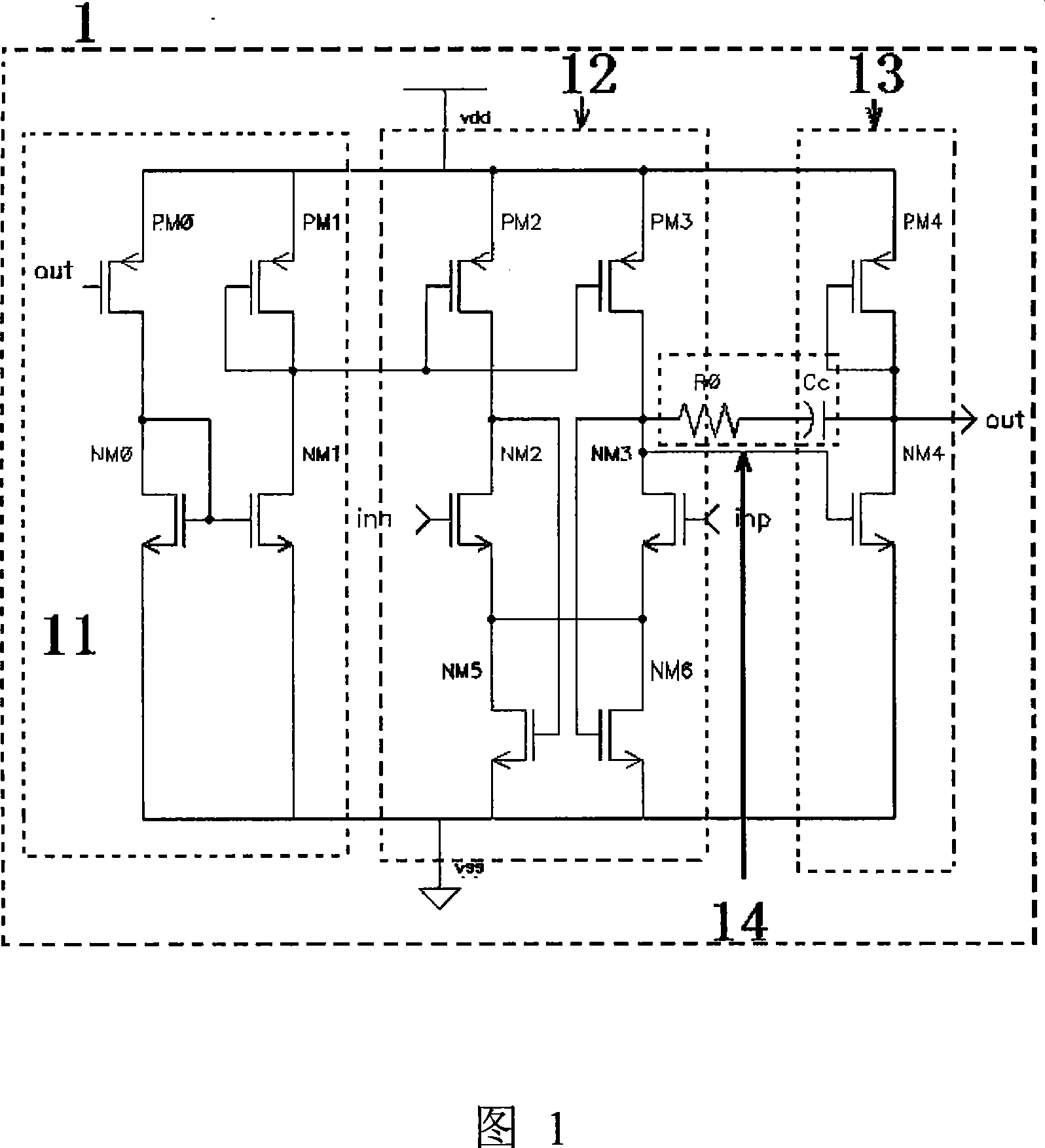
[0030] like figure 1 as shown, figure 1 It is a circuit diagram of a self-biased operational transconductance amplifier provided by the present invention, which is composed of a bias circuit 11, a differential input stage circuit 12, an output stage circuit 13 and a two-stage amplifier compensation circuit 14.

[0031] Wherein, the bias circuit 11 includes PMOS transistors PM0 and PM1, and NMOS transistors NM0 and NM1; wherein, the gate of NM1, the gate and drain of NM0 and the drain of P0 are directly coupled, and the gate and drain of PM1 The drain of NM1 is directly coupled to the gates of PM2 and PM3 in the differential input stage circuit 12, the sources of PM0 and PM1 are connected to the reference power supply, and ...


PUM


Abstract

The invention discloses a circuit of a self-bias low-voltage operational transconductance amplifier with adjustable loop gain and a loop gain control method. The self-bias low-voltage operational transconductance amplifier adopts a self-bias operational transconductance amplifier to provide a two-stage operational transconductance amplifier with a direct current bias, and provide the operational transconductance amplifier circuit with a partial positive feedback mechanism, thereby getting higher gain superior to a traditional operational amplifier; and the circuit gain thereof is controlled at the same time by adjusting the dimension proportion of a tail current tube of a differential input stage, thereby ensuring the stability and obtaining the optimized performance of the operational amplifier.

Description

technical field [0001] The invention relates to the technical field of operational transconductance amplifiers, in particular to a self-biased low-voltage operational transconductance amplifier circuit with controllable loop gain and a loop gain control method. Background technique [0002] With the rapid development of large-scale integrated circuit technology, operational transconductance amplifiers are widely used in various analog and radio frequency integrated circuits. Due to the rapid development of digital mobile communication technology, high-performance operational amplifiers have been widely used in high-speed and high-precision analog-to-digital converters (Analogue-to-Digital Converters, ADCs), and are one of the core unit circuits in high-performance pipeline ADCs. , its performance and power consumption directly affect the overall performance of the A / D converter and the continuous working time of the mobile device. Therefore, the design of operational amplif...

Claims


Application Information

Patent Timeline
Patent Type & Authority Patents(China)
IPC IPC(8): H03F3/45
Inventor 王晗叶青
Owner 灿芯创智微电子技术(北京)有限公司
Why Eureka
Try Eureka