Encapsulation structure and method for semi-conductor

A technology of packaging structure and packaging method, which is applied in the direction of semiconductor devices, semiconductor/solid-state device manufacturing, semiconductor/solid-state device components, etc., and can solve complex problems

Inactive Publication Date: 2009-08-12
叶秀慧
View PDF4 Cites 10 Cited by
  • Summary
  • Abstract
  • Description
  • Claims
  • Application Information

AI Technical Summary

Problems solved by technology

However, the above-mentioned existing technologies still use relatively complicated manufacturing procedures, such as: US Patent No. 7,074,696, which discloses a patterned dielectric layer on the substrate, and then the chip is bonded to the dielectric layer. layer (dielectric layer), and make the contacts on the chip between the patterned dielectric layer, after the substrate is removed, the wiring of the metal wire is directly carried out on the patterned dielectric layer

Method used


Image

  • Encapsulation structure and method for semi-conductor
  • Encapsulation structure and method for semi-conductor
  • Encapsulation structure and method for semi-conductor

Examples


Embodiment Construction

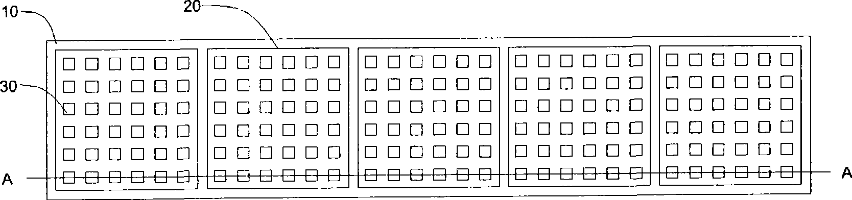
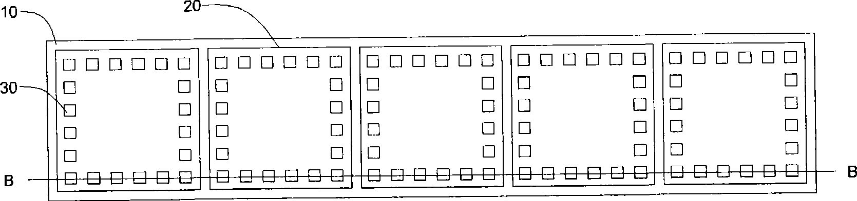
[0016] The subject of the present invention discussed here is a semiconductor packaging structure and its packaging method, especially a ball grid array packaging structure. For a thorough understanding of the present invention, detailed packaging steps will be provided in the following description. Obviously, the practice of the present invention is not limited to the specific details familiar to those skilled in the packaging methods of semiconductor or ball grid array package structures. On the other hand, detailed steps of well-known semiconductor and ball grid array packaging structures and their packaging methods and their subsequent processes are not described in detail to avoid unnecessary limitations on the present invention. However, preferred embodiments of the present invention will be described in detail as follows, and the present invention can be widely used in other embodiments besides these detailed descriptions, and the scope of the present invention is not l...


PUM


Abstract

The invention relates to a ball grid array packaging structure and a packaging method thereof. The packaging structure comprises a circuit board provided with an upper surface and a lower surface. The method comprises the following steps that: firstly, the upper surface is provided with patterned conductive contacts, while the lower surface is provided with corresponding metal endpoints which are electrically connected with the patterned conductive contacts; secondly, a plurality of welding pads on the active surface of a semiconductor chip are electrically connected with the patterned conductive contacts; thirdly, a packaging body is used for coating the semiconductor and the upper surface of the circuit board; and finally, a plurality of conducting elements are electrically connected with the metal endpoints on the lower surface of the circuit board.

Description

technical field [0001] The invention mainly discloses a semiconductor package structure, more particularly a package structure and method for electrically connecting a semiconductor chip with a conductive contact on a carrier to form a ball grid array. Background technique [0002] In recent years, with the continuous maturity and development of semiconductor technology, various high-performance electronic products are constantly being introduced, and the functions of electronic products are developing towards humanization and multi-function. However, there are various functions inside electronic products. integrated circuit (IC) components. In the production process of electronic components, integrated circuit packaging plays a very important role, and integrated circuit packaging can be roughly divided into dual in-line package (DualIn-line Package, DIP), ball grid array package (Ball Grid Array) package, BGA) and tape automatic bonding (Tape Automatic Bonding, TAB) packa...

Claims


Application Information

Patent Timeline
Patent Type & Authority Applications(China)
IPC IPC(8): H01L21/50H01L21/60H01L21/56H01L25/00H01L23/488H01L23/31
CPCH01L24/19H01L24/96H01L21/568H01L2224/12105H01L2224/19H01L2924/14
Inventor 叶秀慧
Owner 叶秀慧
Why Eureka
Try Eureka