Multi-clock system-on-chip with universal clock control modules for transition fault test at speed multi-core

A clock control module and multi-clock technology, which is applied in digital circuit testing, electronic circuit testing, electrical measurement, etc., can solve problems that depend on multi-clock chip-based system design, complexity, etc.

Inactive Publication Date: 2009-08-19
NXP BV
View PDF0 Cites 6 Cited by
  • Summary
  • Abstract
  • Description
  • Claims
  • Application Information

AI Technical Summary

Problems solved by technology

Each of these solutions requires additional development time and effort because these blocks are complex (from a timing closure and clock tree construction perspective) and depend on a multi-clock system-on-chip design

Method used


Image

  • Multi-clock system-on-chip with universal clock control modules for transition fault test at speed multi-core
  • Multi-clock system-on-chip with universal clock control modules for transition fault test at speed multi-core
  • Multi-clock system-on-chip with universal clock control modules for transition fault test at speed multi-core

Examples


Embodiment Construction

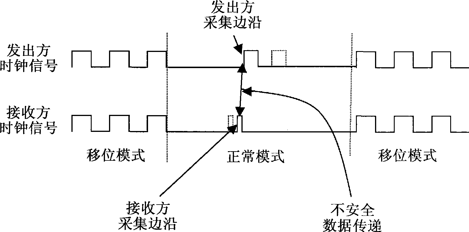
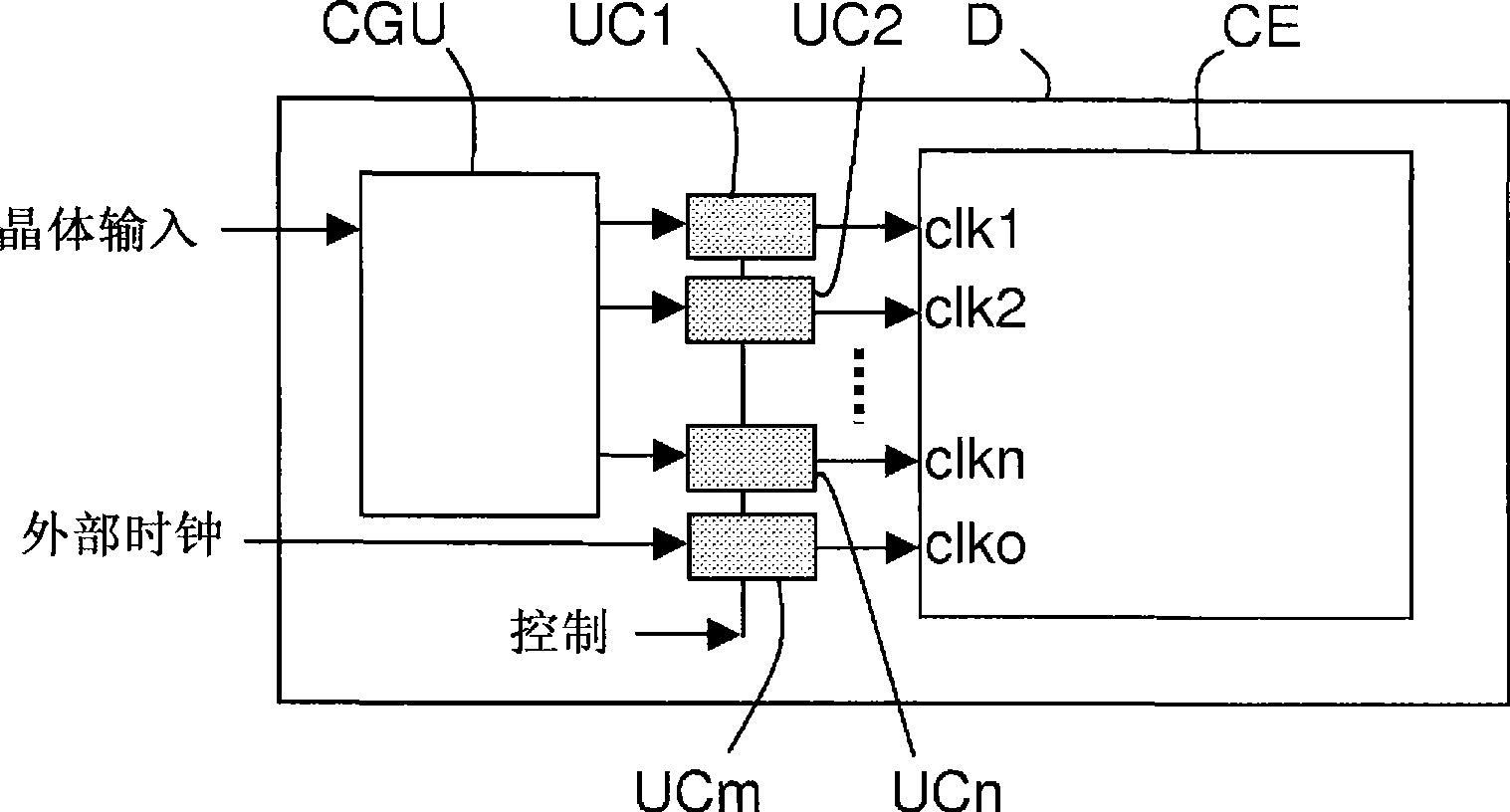
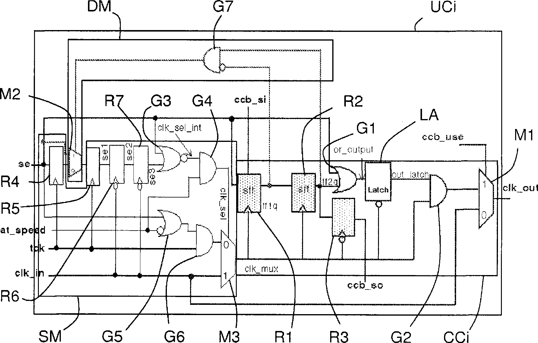
[0019] initial reference figure 2 Let us introduce the multi-clock chip-based system D according to the present invention.

[0020] In the following presentation a multi-clock chip-based system D equipped with an electronic device such as a mobile phone will be considered as an example. However, the present invention is not limited to this type of electronic device (or application). It applies to any type of electronic device that may or may not be suitable for communication (telecommunications) and that requires at least one core (i.e. processor or microcontroller) to execute a program (or software(s)) or commands . So, it could also be eg a Personal Digital Assistant (PDA), a computer (possibly portable), a game or an audio or video player, a television or a set top box.

[0021] Also in the following description, a multi-clock chip-based system D comprising only one core will be considered in order to simplify the description of the invention. However, the present inve...


PUM


Abstract

A multi-clock system-on-chip (D) comprises i) a core (CE) comprising asynchronous clock domains provided for exchanging test data therebetween, ii) a clock generator unit (CGU) arranged for delivering primary clock signals (clkl-clko) for at least some of the clock domains, and iii) clock control modules (CCl-CCo), arranged respectively for defining the functional clock signals from the primary clock signals and from control signals (intended for setting the clock control modules (CCl) in a normal mode allowing test data transmission from the corresponding emitter clock domain to at least one receiver clock domain or a shift mode forbidding such a test data transmission). Each clock control module (CCl) is connected to a synchronisation means (SM) arranged for switching it from the shift mode to the normal mode, and to a delay means (DM) arranged for putting back the emitter launch edge of a functional clock signal intended for the emitter clock domain when this clock control module (CCl) is set into the normal mode, in order this emitter launch edge be temporally located before each corresponding receiver capture edge of the clock signals intended for the receiver clock domains to which the emitter clock domain must transmit test data.

Description

technical field [0001] The present invention relates to a multi-clock chip-based system that allows real-speed transition failure testing. Background technique [0002] A multi-clock chip-based system of the type described above is a component of an electronic device that typically includes i) at least one core (processor or microcontroller or digital IP) including at least two asynchronous clock domains, the two asynchronous clock domains are provided for exchanging (transmitting and / or receiving) test data between each other, ii) a clock generator unit arranged to supply a master clock signal for at least some of the clock domains, and iii) at least two clock control modules (or blocks), respectively arranged for defining a functional clock signal from said master clock signal and from a control signal. The control signal is designed to set the clock control module into a test normal mode enabling test data transfer from the corresponding sender clock domain to at least o...

Claims


Application Information

Patent Timeline
IPC IPC(8): G01R31/3185G01R31/317
CPCG01R31/318552G01R31/31726G01R31/318594G01R31/31727
Inventor 保罗-亨利·普列西-孔蒂埃尔夫·樊尚
Owner NXP BV
Why Eureka
Try Eureka