Electronic part device and method of manufacturing it and electronic part assembly and method of manufacturing it

A technology of electronic components and components, which is applied in the fields of electronic component devices and their manufacturing and electronic component components and their manufacturing, can solve problems such as weak cut-off force, achieve the effect of preventing melting erosion and maintaining reliability

Inactive Publication Date: 2009-08-19
MURATA MFG CO LTD
View PDF1 Cites 7 Cited by
  • Summary
  • Abstract
  • Description
  • Claims
  • Application Information

AI Technical Summary

Problems solved by technology

Therefore, there is a disadvantage that the cutting force is relatively weak

Method used


Image

  • Electronic part device and method of manufacturing it and electronic part assembly and method of manufacturing it
  • Electronic part device and method of manufacturing it and electronic part assembly and method of manufacturing it
  • Electronic part device and method of manufacturing it and electronic part assembly and method of manufacturing it

Examples


Embodiment Construction

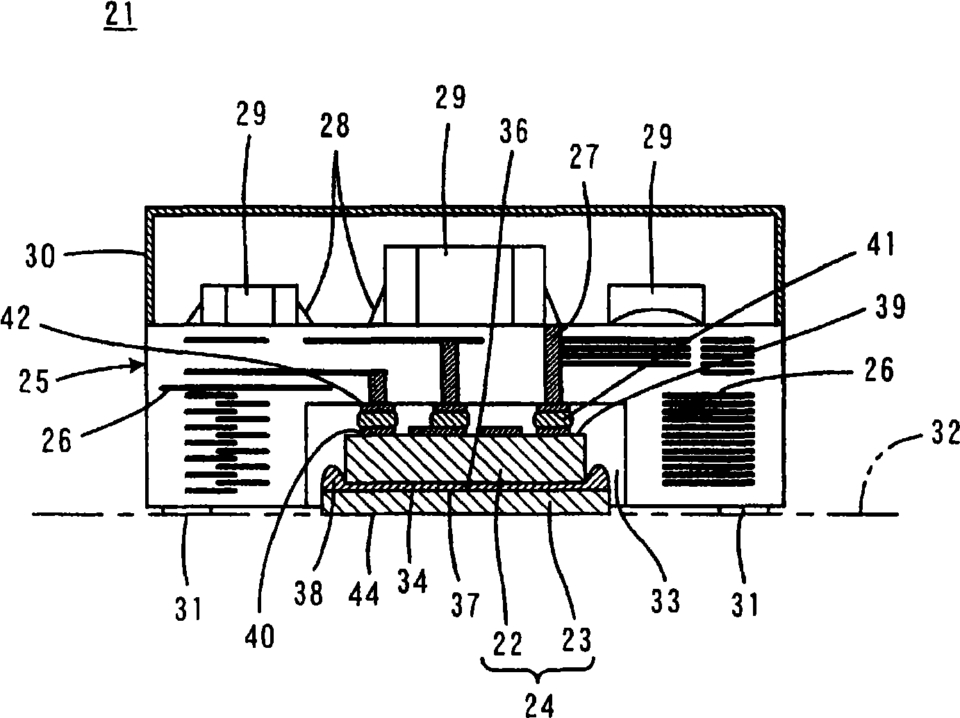
[0057] figure 1 It is a sectional view showing the electronic component module 21 according to one embodiment of the present invention.

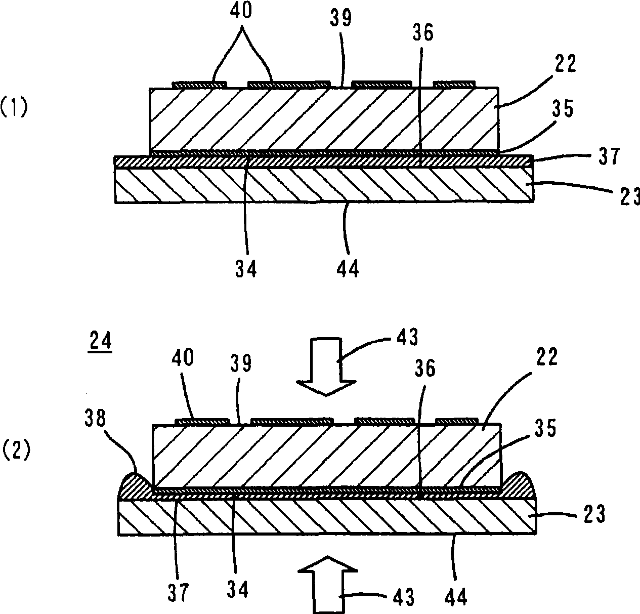
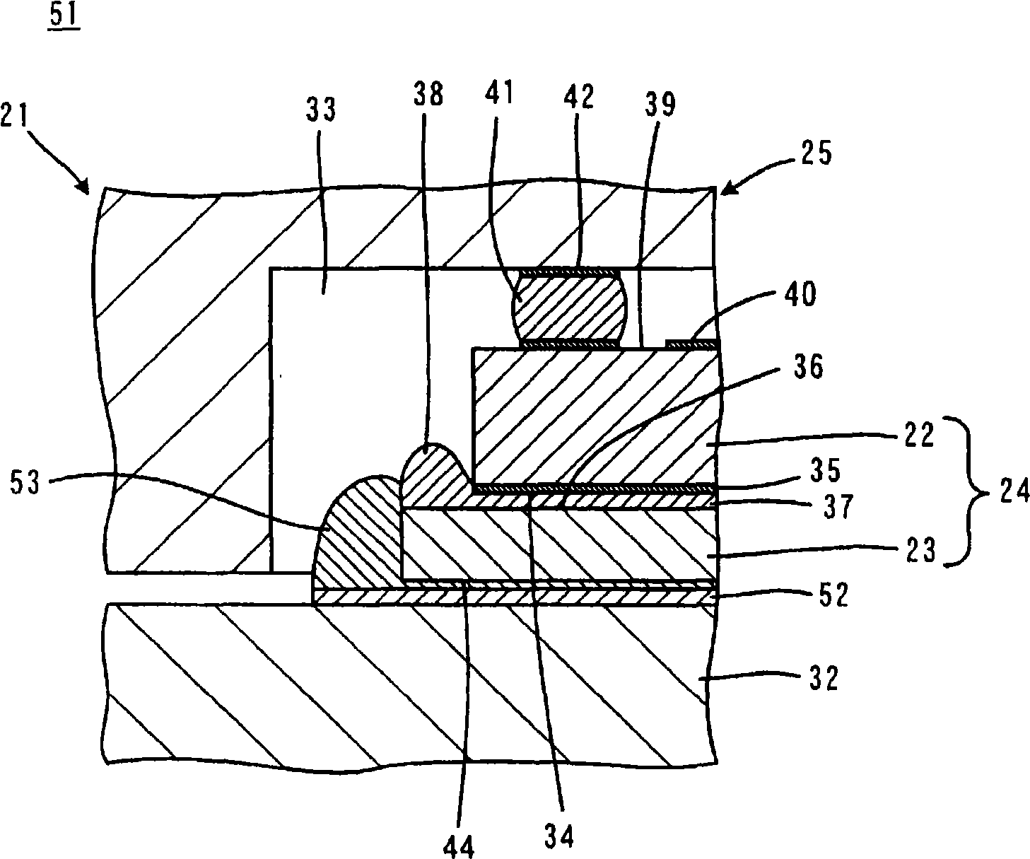
[0058] The electronic component module 21 includes an electronic component device 24 having a structure in which a metal plate 23 and an electronic component element 22 are joined. Furthermore, the electronic component module 21 has a case 25 in which the above-mentioned electronic component device 24 is accommodated.

[0059] The case 25 has a multilayer structure in which a plurality of ceramic layers or organic material layers are laminated, and several internal conductor films 26 and several via conductors 27 are formed inside. Passive components such as inductors, capacitors, and resistors are formed by wiring conductors including these inner conductor films 26 and via-hole conductors 27 .

[0060] On the upper surface of the case 25, if necessary, several external conductor films (not shown.) are formed, and in a state connected to ...


PUM


Abstract

If solder for joining a metal sheet to the metal surface of a board melts and erodes solder for joining an electronic part element to the metal sheet when an electronic part device in which the metal sheet is joined to the electronic part element is mounted on the board, the reliability of joining between the electronic part element and the metal sheet is lowered. A ridge (38) extending along the periphery of the bottom surface (34) of the electronic part element (22) is formed by a part of a first solder (37) for joining the electronic part element (22) to the metal sheet (23). The ridge (38) intercepts a second solder (53) for joining the metal sheet (23) to a board (32) serving as a mother board to prevent the first solder (37), which contributes to the joining of the electronic part element (22) to the metal sheet (23), from being melted and eroded.

Description

technical field [0001] The present invention relates to an electronic component device having a structure in which a metal plate is joined to an electronic component element and a manufacturing method thereof, and an electronic component assembly having a structure in which the electronic component device is mounted on a substrate and a manufacturing method thereof. Background technique [0002] As a technique of interest in the present invention, there is a technique described in JP-A-2003-258192 (Patent Document 1). In Patent Document 1, it is described that the Figure 4 (1) shows this stage, to manufacture Figure 4 The method of the electronic component module 1 shown in (2). [0003] Electronic Components Module 1 as Figure 4 As shown in (2), an electronic component device 4 having a structure in which a metal plate 3 functioning as a heat sink is bonded to the electronic component element 2 is included. Furthermore, the electronic component module 1 includes a case ...

Claims


Application Information

Patent Timeline
Patent Type & Authority Applications(China)
IPC IPC(8): H01L23/40H01L21/52
CPCH01L2924/15738H01L2924/01027H01L24/83H01L2924/01002H01L2924/15724H01L23/4334H01L2924/19105H01L2224/73253H01L2924/15747H01L2224/83194H01L2924/0105H01L2224/83051H01L2924/0132H01L2924/01004H01L2924/1576H01L2224/27013H01L2924/01078H01L23/36H01L2924/19041H01L23/3736H01L2924/01079H01L2224/83801H01L2924/14H01L2224/291H01L23/367H01L2924/01024H01L2924/19042H01L2924/01013H01L23/42H01L25/165H01L2924/16152H01L2224/29111H01L2924/01029H01L2924/19043H01L2924/0133H01L24/32H01L2924/01033H01L2924/15763H01L2224/26175Y10T428/12396H01L2924/01026H01L2924/01028H01L2924/01047H01L2924/00014H01L2924/014
Inventor 北山裕树堀良嗣
Owner MURATA MFG CO LTD
Why Eureka
Try Eureka