

Dc/DC power converting apparatus
A power conversion device and circuit technology, which is applied to output power conversion devices, electrical components, charge balance circuits, etc., can solve problems such as hindering high efficiency and diode conduction loss, and achieve the effect of reducing conduction loss and large power conversion.
- Summary
- Abstract
- Description
- Claims
- Application Information
AI Technical Summary
Problems solved by technology
Method used
Image

Examples
Embodiment approach 1
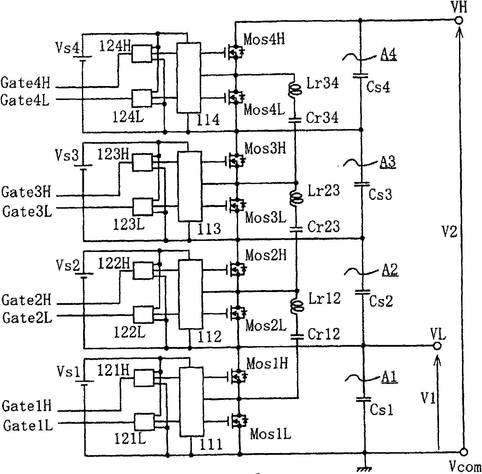
[0039] Hereinafter, a DC / DC power converter according to Embodiment 1 of the present invention will be described with reference to the drawings. figure 1 , figure 2 The circuit configuration of the DC / DC power conversion device according to Embodiment 1 of the present invention is shown, especially figure 1 shows the main part, figure 2 The gate signal generation part is shown.
[0040] like figure 1 As shown, the DC / DC power conversion device has a function of converting the voltage V1 input between the voltage terminals VL and Vcom into a voltage V2 boosted by about 4 times, and outputting it between the voltage terminals VH and Vcom.
[0041] The main circuit part of the DC / DC power conversion device is configured by connecting circuits A1, A2, A3, and A4 in series. The circuits A1, A2, A3, and A4 include smoothing capacitors Cs1, Cs2, Cs3, and Cs4 and a plurality of MOSFETs. The smoothing capacitors Cs1, Cs2, Cs3, and Cs4 smooth the input and output voltages V1, V2, ...
Embodiment approach 2
[0073] In Embodiment 1 above, a step-up DC / DC power converter that boosts the voltage V1 to approximately four times the voltage V2 was shown, but in this embodiment, the step-down from the voltage V2 to the voltage V2 is shown. Step-down DC / DC power conversion device of V1.
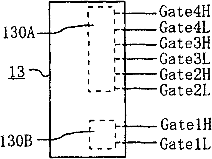
[0074] The main part of the circuit configuration of the DC / DC power converter of the present embodiment and figure 1 The shown circuit configurations are the same, but in this case, the circuit A4 is used for the drive inverter circuit, and the circuits A1, A2, and A3 are used for the rectifier circuit. In addition, the control circuit 13a as the gate signal generation part is different from the above-mentioned first embodiment, as Figure 5 shown.
[0075] like Figure 5 As shown, gate signals Gate1L, Gate1H, Gate2L, Gate2H, Gate3L, Gate3H, Gate4L, Gate4H are generated in the control circuit 13a. In the control circuit 13a, there are: a drive gate signal generation section 130B for generating drive...
Embodiment approach 3
[0106] The step-up DC / DC power converter of V1→V2 is shown in the first embodiment above, and the step-down DC / DC power converter of V2→V1 is shown in the second embodiment above, but in this embodiment In the form, a buck-boost type DC / DC power conversion device is shown which realizes bidirectional energy transfer by having the functions of Embodiments 1 and 2 described above at the same time.
[0107] The main part of the circuit configuration of the DC / DC power converter of this embodiment is the same as that of the first and second embodiments described above. figure 1 The circuit configuration shown in , in this case, circuit A1 is used as an inverter circuit for driving when boosting voltage, circuits A2, A3, and A4 are used as a rectifier circuit, and circuit A4 is used as a driving circuit when voltage is lowered. Using the inverter circuit, use the circuits A1, A2, A3 for the rectification circuit. In addition, the control circuit 13b as the gate signal generation p...
PUM
 Abstract
Description
Claims
Application Information