
Resistance-type touch screen and manufacturing method thereof
A touch screen and resistive technology, which is applied in the field of resistive touch screen and its production, can solve the problems of complex manufacturing process of resistive touch screen, achieve the effects of saving manpower and material resources, shortening the process flow and improving product yield
- Summary
- Abstract
- Description
- Claims
- Application Information
AI Technical Summary
Problems solved by technology
Method used
Image

Examples
Embodiment Construction
[0023] In order to make the object, technical solution and advantages of the present invention clearer, the present invention will be further described in detail below in conjunction with the accompanying drawings and embodiments. It should be understood that the specific embodiments described here are only used to explain the present invention, not to limit the present invention.
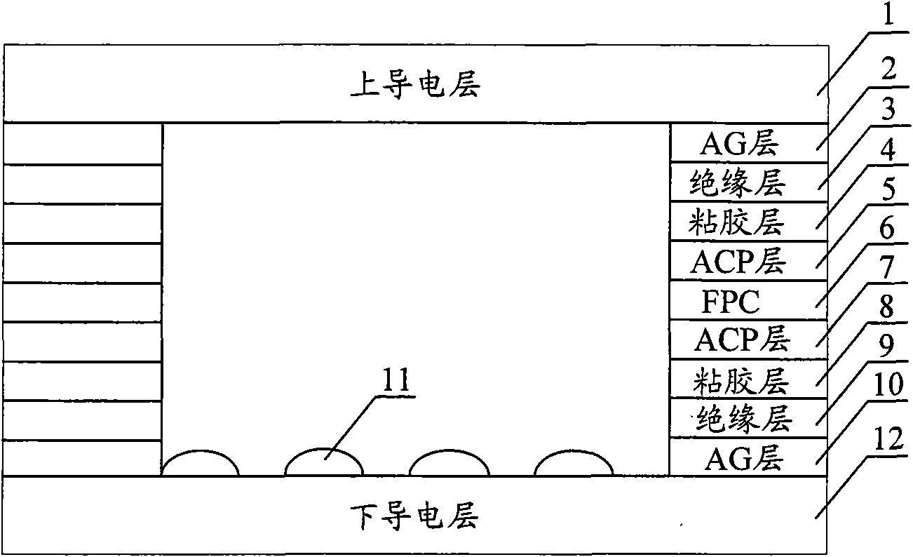
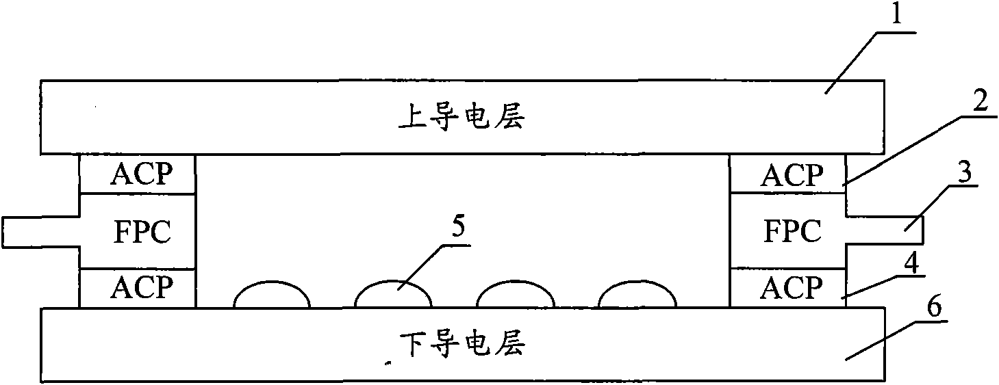
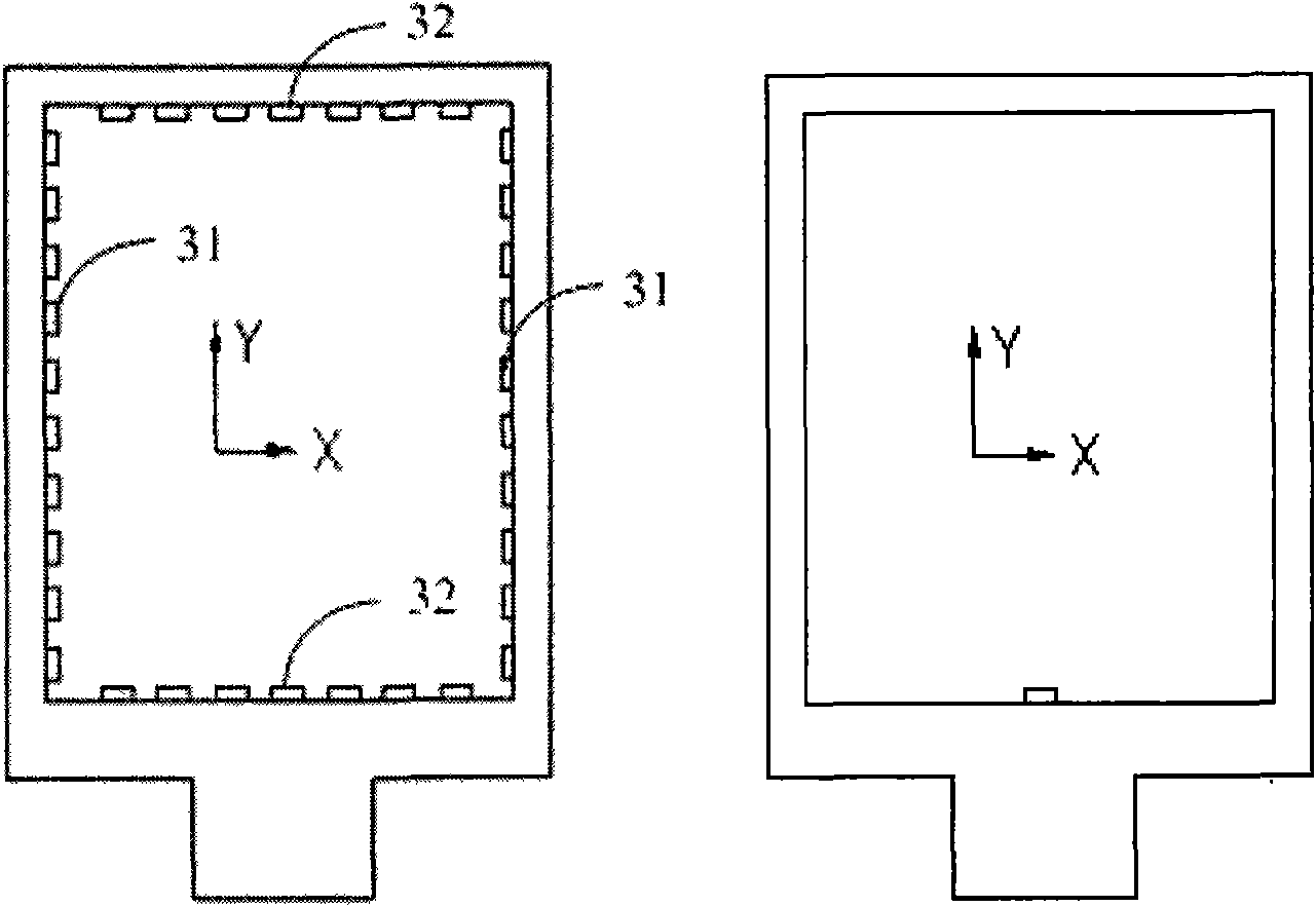
[0024] The resistive touch screen provided by the embodiment of the present invention only needs upper and lower conductive layers, isolation points and a flexible printed circuit board in structure, and the lower conductive layer is used as a voltage distribution layer, with isolation points attached to one side, and the flexible printed circuit board is located on the lower conductive layer. The side of the isolation point is electrically connected to the lower conductive layer, and the upper conductive layer is used to detect voltage and bonded to the flexible printed circuit board. The manufactu...
PUM
 Abstract
Description
Claims
Application Information