Full-custom AES SubByte circuit resisting differential power analysis attack

A differential power consumption analysis and fully customized technology, applied in logic circuits, encryption devices with shift registers/memory, electrical components, etc., can solve problems such as lack of security of SubByte

Inactive Publication Date: 2009-09-09
FUDAN UNIV
View PDF0 Cites 12 Cited by
  • Summary
  • Abstract
  • Description
  • Claims
  • Application Information

AI Technical Summary

Problems solved by technology

Therefore, the design of SubByte based on scCMOS

Method used


Image

  • Full-custom AES SubByte circuit resisting differential power analysis attack
  • Full-custom AES SubByte circuit resisting differential power analysis attack
  • Full-custom AES SubByte circuit resisting differential power analysis attack

Examples


Embodiment Construction

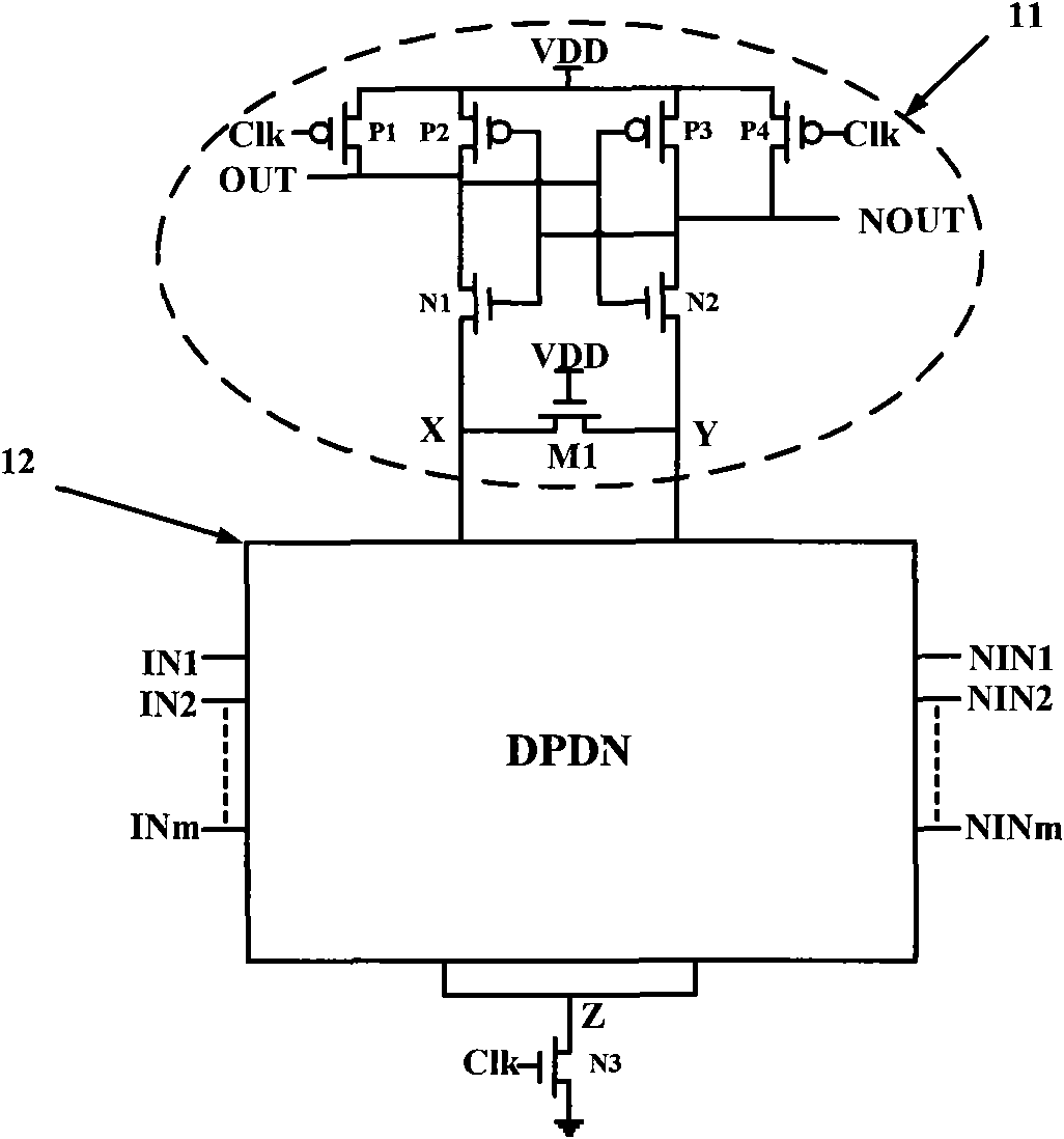
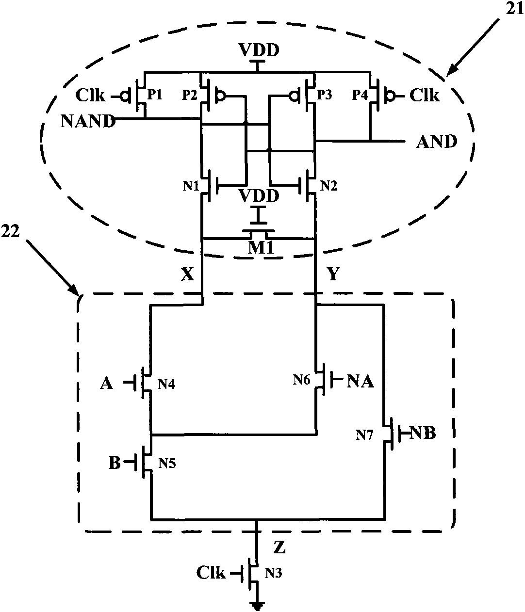
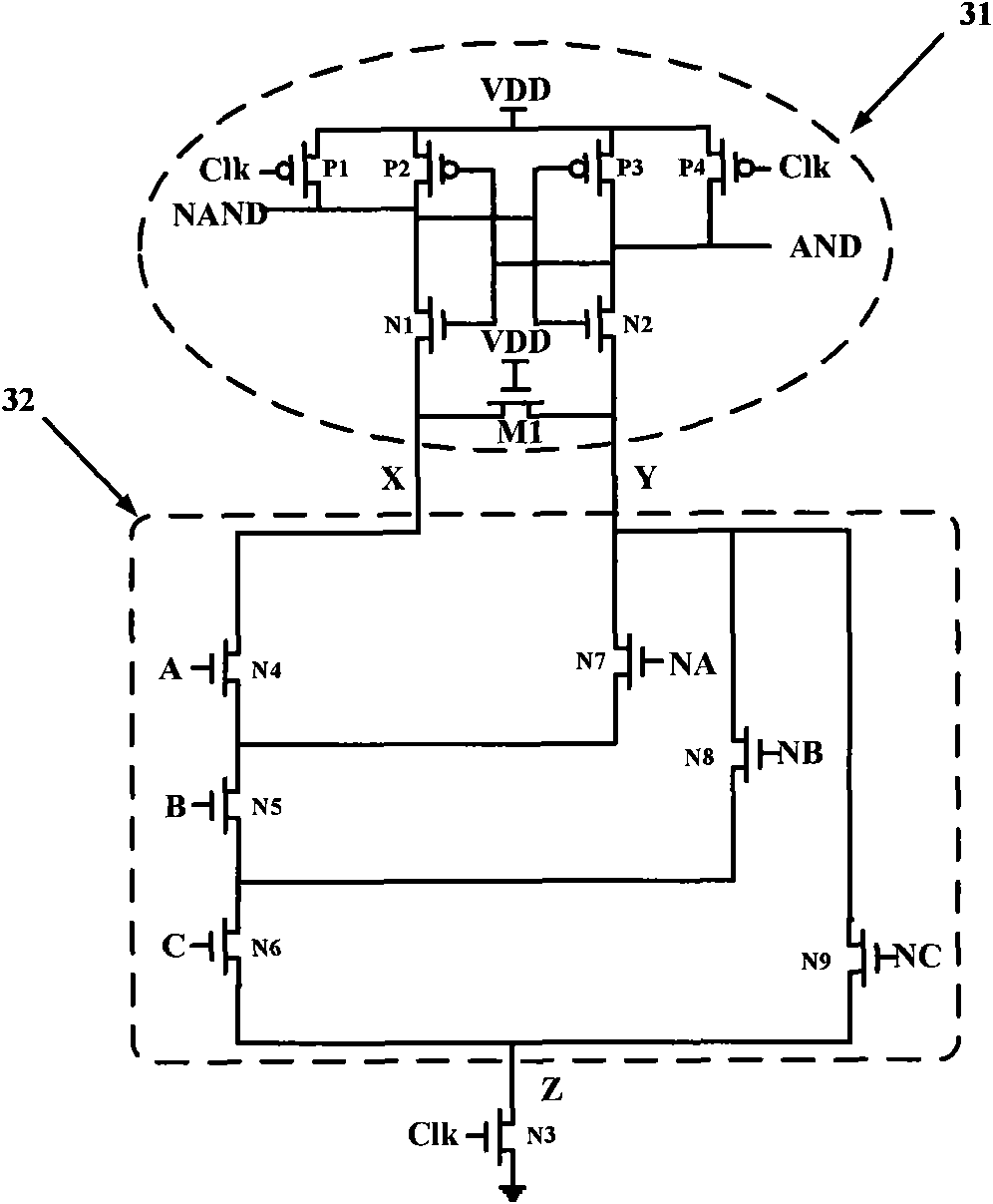
[0024] The purpose of the present invention is to propose a fully customized AES SubByte circuit that is resistant to differential power analysis attacks, so that the AESS SubByte module structure is resistant to differential power analysis attacks, embedded in AES, and can make the entire AES structure resistant to differential power analysis.

[0025] The SubByte structure is the most complicated part of the AES algorithm. It contains non-linear operations and has different affine transformations for encryption and decryption. There are two implementation methods of the SubByte module, one is a lookup table, and the other is a finite field operation. In order to reduce the hardware area, the present invention adopts the method of finite field calculation to realize the SubByte module. About to be originally in GF(2 8 ) domain inverse calculation, converted to GF(2 4 ) domain implementation. Since GF(2 4 ) field is relatively simple, and can quickly and effectively perfo...


PUM


Abstract

The invention belongs to the technical field of the design of information security chips, in particular to a full-custom AES (advanced encryption standard) SubByte circuit resisting differential power analysis attack. The AES SubByte circuit is realized by the following basic units: a reactor INV, two input sensitive amplifier AND gates (AND2D1), three input sensitive amplifier AND gates (AND3D1), two input sensitive amplifier XOR gates (XOR2D1), and three input sensitive amplifier XOR gates (XOR3D1). The circuit uses a streamline structure to substitute the direct connection, and obtains higher speed with smaller area, and an adopted latch is a sense amplifier flip-flop. The circuit can realize the independency of power consumption of the circuit, operational data and operating sequence, thereby effectively preventing the differential power analysis attack. The circuit adopts an SMIC 0.18mu m CMOS process, the working frequency of the circuit achieves 83.3MHz, and the chip area of the circuit is about 0.85mm<2>. The circuit can be widely applied to symmetrical encryption operation equipment with high security.

Description

technical field [0001] The invention belongs to the technical field of information security chip design, and in particular relates to a byte replacement (AES SubByte) circuit of a fully customized advanced cryptographic algorithm resistant to differential power analysis attacks. Background technique [0002] Advanced Encryption Standard (AES) is a commonly used symmetric encryption algorithm proposed by NIST (National Institute of Standards and Technology). Cryptographic chips using this algorithm are widely used in smart cards, e-commerce, online banking and other fields, which greatly guarantee the security of the system. But in recent years, attackers have been able to find the keys of cryptographic chips through side-channel information leaked by digital CMOS gate jumps. In particular, differential power analysis (Differential Power Analysis, DPA) attacks can find keys very effectively by analyzing power consumption characteristics generated by data transitions. In the...

Claims


Application Information

Patent Timeline
IPC IPC(8): H04L9/06H03K19/0948
Inventor 韩军李亮曾晓洋赵佳
Owner FUDAN UNIV
Why Eureka
Try Eureka